- 您現在的位置:買賣IC網 > PDF目錄385422 > HY57V643220CLT-5 (HYNIX SEMICONDUCTOR INC) 4 Banks x 512K x 32Bit Synchronous DRAM PDF資料下載
參數資料
| 型號: | HY57V643220CLT-5 |
| 廠商: | HYNIX SEMICONDUCTOR INC |
| 元件分類: | DRAM |
| 英文描述: | 4 Banks x 512K x 32Bit Synchronous DRAM |
| 中文描述: | 2M X 32 SYNCHRONOUS DRAM, 4.5 ns, PDSO86 |
| 封裝: | 0.400 X 0.875 INCH, 0.5 MM PITCH, TSOP2-86 |
| 文件頁數: | 1/12頁 |
| 文件大?。?/td> | 183K |
| 代理商: | HY57V643220CLT-5 |
HY57V643220C
4 Banks x 512K x 32Bit Synchronous DRAM
This document is a general product description and is subject to change without notice. Hynix Semiconductor does not assume any
responsibility for use of circuits described. No patent licenses are implied.
Rev. 0.8/Aug. 02 1
DESCRIPTION
The Hynix HY57V643220C is a 67,108,864-bit CMOS Synchronous DRAM, ideally suited for the memory applications
which require wide data I/O and high bandwidth. HY57V643220C is organized as 4banks of 524,288x32.
HY57V643220C is offering fully synchronous operation referenced to a positive edge of the clock. All inputs and out-
puts are synchronized with the rising edge of the clock input. The data paths are internally pipelined to achieve very
high bandwidth. All input and output voltage levels are compatible with LVTTL.
Programmable options include the length of pipeline (Read latency of 2 or 3), the number of consecutive read or write
cycles initiated by a single control command (Burst length of 1,2,4,8 or full page), and the burst count
sequence(sequential or interleave). A burst of read or write cycles in progress can be terminated by a burst terminate
command or can be interrupted and replaced by a new burst read or write command on any cycle. (This pipelined
design is not restricted by a `2N` rule.)
FEATURES
JEDEC standard 3.3V power supply
All device pins are compatible with LVTTL interface
JEDEC standard 400mil 86pin TSOP-II with 0.5mm of
pin pitch
All inputs and outputs referenced to positive edge of
system clock
Data mask function by DQM0,1,2 and 3
Internal four banks operation
Auto refresh and self refresh
4096 refresh cycles / 64ms
Programmable Burst Length and Burst Type
- 1, 2, 4, 8 or full page for Sequential Burst
- 1, 2, 4 or 8 for Interleave Burst
Programmable CAS Latency ; 2, 3 Clocks
Burst Read Single Write operation
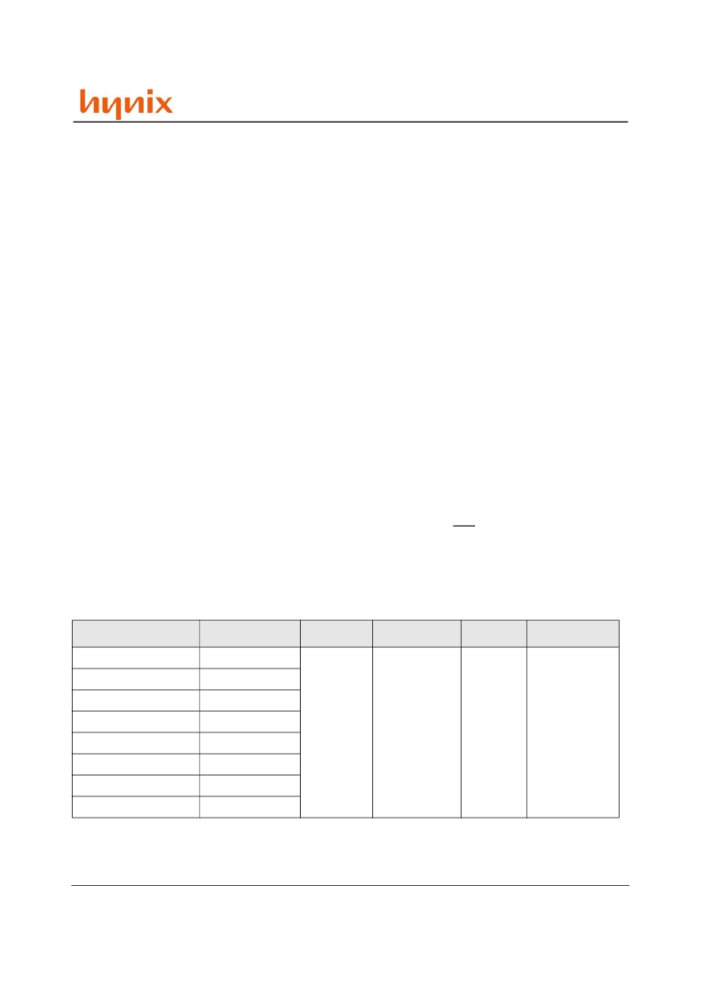
ORDERING INFORMATION
Part No.
Clock Frequency
Power
Organization
Interface
Package
HY57V643220C(L)T-47
212MHz
Normal/
Low Power
4Banks x
512Kbits x32
LVTTL
400mil 86pin
TSOP II
HY57V643220C(L)T-5
200MHz
HY57V643220C(L)T-55
183MHz
HY57V643220C(L)T-6
166MHz
HY57V643220C(L)T-7
143MHz
HY57V643220C(L)T-8
125MHz
HY57V643220C(L)T-P
100MHz
HY57V643220C(L)T-S
100MHz
相關PDF資料 |
PDF描述 |
|---|---|
| HY57V643220CLT-55 | 4 Banks x 512K x 32Bit Synchronous DRAM |
| HY57V643220CLT-6 | 4 Banks x 512K x 32Bit Synchronous DRAM |
| HY57V643220CLT-7 | 4 Banks x 512K x 32Bit Synchronous DRAM |
| HY57V643220CLT-8 | 4 Banks x 512K x 32Bit Synchronous DRAM |
| HY57V643220D | 4Banks x 512K x 32bits Synchronous DRAM |
相關代理商/技術參數 |
參數描述 |
|---|---|
| HY57V643220CLT-55 | 制造商:HYNIX 制造商全稱:Hynix Semiconductor 功能描述:4 Banks x 512K x 32Bit Synchronous DRAM |
| HY57V643220CLT-55I | 制造商:未知廠家 制造商全稱:未知廠家 功能描述:SDRAM|4X512KX32|CMOS|TSSOP|86PIN|PLASTIC |
| HY57V643220CLT-5I | 制造商:未知廠家 制造商全稱:未知廠家 功能描述:x32 SDRAM |
| HY57V643220CLT-6 | 制造商:HYNIX 制造商全稱:Hynix Semiconductor 功能描述:4 Banks x 512K x 32Bit Synchronous DRAM |
| HY57V643220CLT-6I | 制造商:未知廠家 制造商全稱:未知廠家 功能描述:SDRAM|4X512KX32|CMOS|TSSOP|86PIN|PLASTIC |
發布緊急采購,3分鐘左右您將得到回復。