- 您現(xiàn)在的位置:買賣IC網(wǎng) > PDF目錄360746 > ICS2509 3.3V Phase-Lock Loop Clock Driver PDF資料下載
參數(shù)資料
| 型號: | ICS2509 |
| 英文描述: | 3.3V Phase-Lock Loop Clock Driver |
| 中文描述: | 3.3鎖相環(huán)時鐘驅(qū)動器 |
| 文件頁數(shù): | 1/7頁 |
| 文件大小: | 248K |
| 代理商: | ICS2509 |
Integrated
Circuit
Systems, Inc.
General Description
The ICS2509C
is a high performance, low skew, low jitter
clock driver. It uses a phase lock loop (PLL) technology to
align, in both phase and frequency, the CLKIN signal with
the CLKOUT signal. It is specifically designed for use with
synchronous SDRAMs. The
ICS2509C
operates at 3.3V VCC
and drives up to nine clock loads.
Features
Meets or exceeds PC133 registered DIMM
specification 1.1
Spread Spectrum Clock Compatible
Distributes one clock input to one bank of five and one
bank of four outputs
Separate output enable(OEA,OEB) for each output bank
Operating frequency 25 MHz to 175 Mhz
External feedback input (FBIN) terminal is used to
synchrionize the outputs to the clock input
No external RC network required
Operates at 3.3V Vcc
Plastic 24-pin 173mil TSSOP package
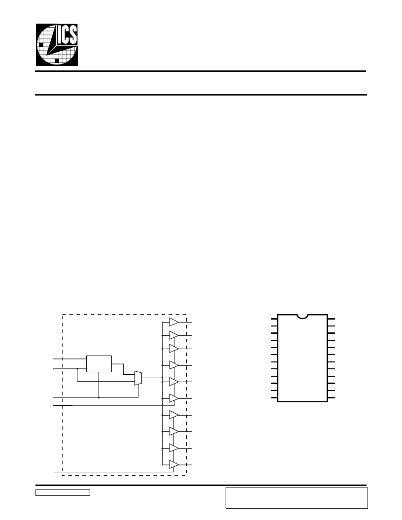
ICS2509C
Block Diagram
3.3V Phase-Lock Loop Clock Driver
2509 C Rev C 06/15/01
Pin Configuration
24 Pin TSSOP
4.40 mm. Body, 0.65 mm. pitch
One bank of five outputs and one bank of four outputs provide
nine low-skew, low-jitter copies of CLKIN. Output signal
duty cycles are adjusted to 50 percent, independent of the
duty cycle at CLKIN. Each bank of outputs can be enabled or
disabled separately via control (OEA and OEB) inputs. When
the OE inputs are high, the outputs align in phase and
frequency with CLKIN; when the OE inputs are low, the
outputs are disabled to the logic low state.
The
ICS2509C
does not require external RC filter
components. The loop filter for the PLL is included on-chip,
minimizing component count, board space, and cost. The
buffer mode shuts off the PLL and connects the input directly
to the output buffer. This buffer mode, the
ICS2509C
can be
use as low skew fanout clock buffer device. The
ICS2509C
comes in 24 pin 173mil Thin Shrink Small-Outline package
(TSSOP) package.
FBIN
CLKIN
AVCC
OEA
OEB
PLL
CLKA0
FBOUT
CLKA1
CLKA2
CLKA3
CLKA4
CLKB0
CLKB1
CLKB2
CLKB3
AGND
VCC
CLKA0
CLKA1
CLKA2
GND
GND
CLKA3
CLKA4
VCC
OEA
FBOUT
CLKIN
AVCC
VCC
CLKB0
CLKB1
GND
GND
CLKB2
CLKB3
VCC
OEB
FBIN
I
1
2
3
4
5
6
7
8
9
10
11
12
24
23
22
21
20
19
18
17
16
15
14
13
ICS reserves the right to make changes in the device data identified in
this publication without further notice. ICS advises its customers to
obtain the latest version of all device data to verify that any
information being relied upon by the customer is current and accurate.
相關(guān)PDF資料 |
PDF描述 |
|---|---|
| ICS2509C | 3.3V Phase-Lock Loop Clock Driver |
| ICS2509CyG-T | 3.3V Phase-Lock Loop Clock Driver |
| ICS2510CG-T | 3.3V Phase-Lock Loop Clock Driver |
| ICS2510C | 3.3V Phase-Lock Loop Clock Driver |
| ICS2572 | User-Programmable Dual High-Performance Clock Generator |
相關(guān)代理商/技術(shù)參數(shù) |
參數(shù)描述 |
|---|---|
| ICS2509C | 制造商:ICS 制造商全稱:ICS 功能描述:3.3V Phase-Lock Loop Clock Driver |
| ICS2509CYG-T | 制造商:ICS 制造商全稱:ICS 功能描述:3.3V Phase-Lock Loop Clock Driver |
| ICS251 | 制造商:IDT 制造商全稱:Integrated Device Technology 功能描述:FIELD PROGRAMMABLE SS VERSACLOCK SYNTHESIZER |
| ICS2510C | 制造商:ICS 制造商全稱:ICS 功能描述:3.3V Phase-Lock Loop Clock Driver |
| ICS2510CG | 功能描述:IC CLOCK DVR PLL 3.3V 24-TSSOP RoHS:否 類別:集成電路 (IC) >> 時鐘/計時 - 時鐘發(fā)生器,PLL,頻率合成器 系列:- 標準包裝:2,000 系列:- 類型:PLL 時鐘發(fā)生器 PLL:帶旁路 輸入:LVCMOS,LVPECL 輸出:LVCMOS 電路數(shù):1 比率 - 輸入:輸出:2:11 差分 - 輸入:輸出:是/無 頻率 - 最大:240MHz 除法器/乘法器:是/無 電源電壓:3.135 V ~ 3.465 V 工作溫度:0°C ~ 70°C 安裝類型:表面貼裝 封裝/外殼:32-LQFP 供應(yīng)商設(shè)備封裝:32-TQFP(7x7) 包裝:帶卷 (TR) |
發(fā)布緊急采購,3分鐘左右您將得到回復。