- 您現在的位置:買賣IC網 > PDF目錄67685 > ICS570MI (INTEGRATED DEVICE TECHNOLOGY INC) 570 SERIES, PLL BASED CLOCK DRIVER, 2 TRUE OUTPUT(S), 0 INVERTED OUTPUT(S), PDSO8 PDF資料下載
參數資料
| 型號: | ICS570MI |
| 廠商: | INTEGRATED DEVICE TECHNOLOGY INC |
| 元件分類: | 時鐘及定時 |
| 英文描述: | 570 SERIES, PLL BASED CLOCK DRIVER, 2 TRUE OUTPUT(S), 0 INVERTED OUTPUT(S), PDSO8 |
| 封裝: | 0.150 INCH, SOIC-8 |
| 文件頁數: | 1/11頁 |
| 文件大小: | 250K |
| 代理商: | ICS570MI |
DATASHEET
MULTIPLIER AND ZERO DELAY BUFFER
ICS570
IDT / ICS MULTIPLIER AND ZERO DELAY BUFFER
1
ICS570
REV K 073007
Description
The ICS570 is a high-performance Zero Delay Buffer (ZDB)
which integrates IDT’s proprietary analog/digital Phase
Locked Loop (PLL) techniques. The A version is
recommended for 5 V designs and the B version for
3.3 V designs. The chip is part of IDT’s ClockBlocksTM
family, and was designed as a performance upgrade to
meet today’s higher speed and lower voltage requirements.
The zero delay feature means that the rising edge of the
input clock aligns with the rising edges of both output
clocks, giving the appearance of no delay through the
device. There are two outputs on the chip, one being a
low-skew divide by two of the other output. The device
incorporates an all-chip power down/tri-state mode that
stops the internal PLL and puts both outputs into a high
impedance state.
The ICS570 is ideal for synchronizing outputs in a large
variety of systems, from personal computers to data
communications to graphics/video. By allowing off-chip
feedback paths, the device can eliminate the delay through
other devices.
The ICS570 A and B versions were designed to improve
input to output jitter from the original ICS570M version, and
are recommended for all new designs.
Features
8-pin SOIC package
Available in Pb (lead) free package
Pin-for-pin replacement and upgrade to ICS570M
Functional equivalent to AV9170 (not a pin-for-pin
replacement)
Low input to output skew of 300 ps max (>60 MHz
outputs)
Ability to choose between 14 different multipliers from
0.5x to 32x
Output clock frequency up to 170 MHz at 3.3 V
Can recover degraded input clock duty cycle
Output clock duty cycle of 45/55
Power Down and Tri-State Mode
Passes spread spectrum clock modulation
Full CMOS clock swings with 25 mA drive capability at
TTL levels
Advanced, low power CMOS process
ICS570B has an operating voltage of 3.3 V (±5%)
ICS570A has an operating voltage of 5.0 V (±5%)
Industrial temperature version available
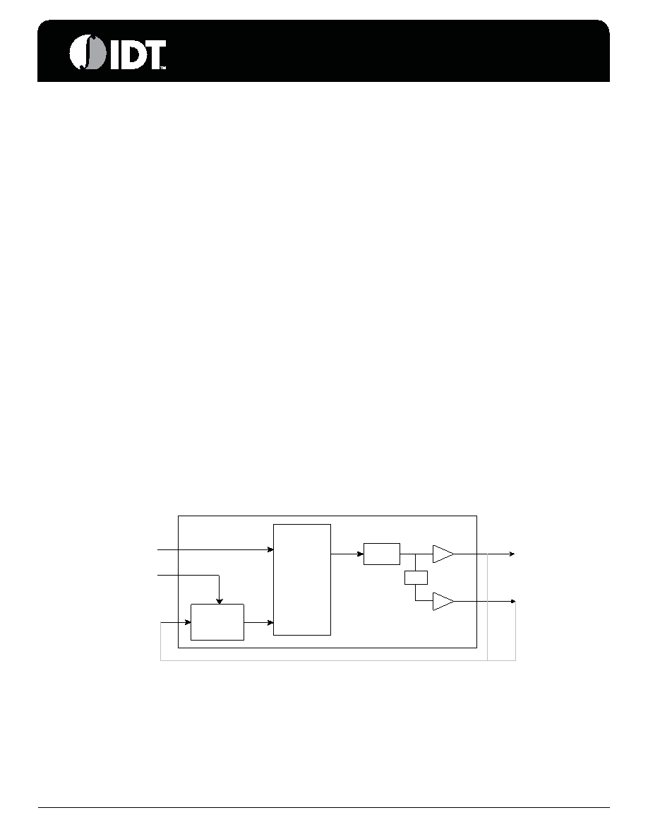
Block Diagram
Ph as e
Detec tor,
C harge
Pum p,
and Loop
F ilter
divide
by N
CL K
E xte rn al fe ed ba ck ca n c o m e from C L K or C L K /2 (s ee ta b le on pa ge 2 )
IC L K
FBIN
S1 :0
VC O
CL K 2
/2
相關PDF資料 |
PDF描述 |
|---|---|
| ICS570MLF | 570 SERIES, PLL BASED CLOCK DRIVER, 2 TRUE OUTPUT(S), 0 INVERTED OUTPUT(S), PDSO8 |
| ICS570AT | 570 SERIES, PLL BASED CLOCK DRIVER, 2 TRUE OUTPUT(S), 0 INVERTED OUTPUT(S), PDSO8 |
| ICS570MT | 570 SERIES, PLL BASED CLOCK DRIVER, 2 TRUE OUTPUT(S), 0 INVERTED OUTPUT(S), PDSO8 |
| ICS650GI-41LF | 50 MHz, PROC SPECIFIC CLOCK GENERATOR, PDSO16 |
| ICS7152AMI-11LF | 67 MHz, OTHER CLOCK GENERATOR, PDSO8 |
相關代理商/技術參數 |
參數描述 |
|---|---|
| ICS570MIT | 制造商:ICS 制造商全稱:ICS 功能描述:Multiplier and Zero Delay Buffer |
| ICS570MT | 制造商:ICS 制造商全稱:ICS 功能描述:Multiplier and Zero Delay Buffer |
| ICS571 | 制造商:ICS 制造商全稱:ICS 功能描述:Low Phase Noise Zero Delay Buffer |
| ICS571M | 功能描述:IC MULTIPLIER/ZDB 8-SOIC RoHS:否 類別:集成電路 (IC) >> 時鐘/計時 - 時鐘發生器,PLL,頻率合成器 系列:ClockBlocks™ 產品變化通告:Product Discontinuation 04/May/2011 標準包裝:96 系列:- 類型:時鐘倍頻器,零延遲緩沖器 PLL:帶旁路 輸入:LVTTL 輸出:LVTTL 電路數:1 比率 - 輸入:輸出:1:8 差分 - 輸入:輸出:無/無 頻率 - 最大:133.3MHz 除法器/乘法器:是/無 電源電壓:3 V ~ 3.6 V 工作溫度:0°C ~ 70°C 安裝類型:表面貼裝 封裝/外殼:16-TSSOP(0.173",4.40mm 寬) 供應商設備封裝:16-TSSOP 包裝:管件 其它名稱:23S08-5HPGG |
| ICS571MLF | 功能描述:IC ZDB LOW PHASE NOISE 8-SOIC RoHS:是 類別:集成電路 (IC) >> 時鐘/計時 - 時鐘發生器,PLL,頻率合成器 系列:ClockBlocks™ 標準包裝:2,000 系列:- 類型:PLL 頻率合成器 PLL:是 輸入:晶體 輸出:時鐘 電路數:1 比率 - 輸入:輸出:1:1 差分 - 輸入:輸出:無/無 頻率 - 最大:1GHz 除法器/乘法器:是/無 電源電壓:4.5 V ~ 5.5 V 工作溫度:-20°C ~ 85°C 安裝類型:表面貼裝 封裝/外殼:16-LSSOP(0.175",4.40mm 寬) 供應商設備封裝:16-SSOP 包裝:帶卷 (TR) 其它名稱:NJW1504V-TE1-NDNJW1504V-TE1TR |
發布緊急采購,3分鐘左右您將得到回復。