- 您現(xiàn)在的位置:買賣IC網(wǎng) > PDF目錄360768 > ICS843004-02 CRYSTAL-TO-3.3V LVPECL FREQUENCY SYNTHESIZER PDF資料下載
參數(shù)資料
| 型號: | ICS843004-02 |
| 英文描述: | CRYSTAL-TO-3.3V LVPECL FREQUENCY SYNTHESIZER |
| 中文描述: | 水晶到3.3的LVPECL頻率合成器 |
| 文件頁數(shù): | 1/12頁 |
| 文件大小: | 185K |
| 代理商: | ICS843004-02 |
843004AG-02
www.icst.com/products/hiperclocks.html
REV. A JULY 20, 2005
1
Integrated
Circuit
Systems, Inc.
ICS843004-02
C
RYSTAL
-
TO
-3.3V LVPECL
F
REQUENCY
S
YNTHESIZER
PRELIMINARY
G
ENERAL
D
ESCRIPTION
The ICS843004-02 is a 4 output LVPECL
Synthesizer optimized to generate clock
frequencies for a variety of high performance
applications and is a member of the
HiPerClocks
TM
family of high performance clock
solutions from ICS. This device can select its input reference
clock from either a crystal input or a single-ended clock signal
and can be configured to generate a number of different output
frequencies via the 3 frequency select pins (F_SEL2:0). The
ICS843004-02 uses ICS’ 3rd generation low phase noise VCO
technology and can achieve 1ps or lower typical rms phase
jitter. This ensures that it will easily meet clocking requirements
for high-speed communication protocols such as 10 and 12
Gigabit Ethernet, 10 Gigbit Fibre Channel, and SONET. This
device is also suitable for next generation serial I/O
technologies like serial ATA and SCSI and is conveniently
packaged in a small 24-pin TSSOP package.
F
EATURES
Four 3.3V LVPECL outputs
Selectable crystal oscillator interface
or LVCMOS/LVTTL single-ended input
Crystal input range: 14MHz - 37.78MHz
VCO Range: 560MHz - 680MHz
Supports the following applications:
SONET, Ethernet, Serial ATA, SCSI and HDTV
RMS phase jitter @ 155.52MHz (12kHz - 20MHz):
0.91ps (typical)
Offset
100Hz ............... -97.1 dBc/Hz
1kHz ..............-121.6 dBc/Hz
10kHz ..............-124.9 dBc/Hz
100kHz ..............-125.1 dBc/Hz
Noise Power
Full 3.3V supply mode
0°C to 70°C ambient operating temperature
HiPerClockS
ICS
P
IN
A
SSIGNMENT
0
1
0
1
Phase
Detector
VCO
÷18
÷24
÷32
(default)
÷40
N
÷1
÷2
÷3
÷4
(default)
÷8
M
OSC
3
ICS843004-02
24-Lead TSSOP
4.40mm x 7.8mm x 0.92mm
package body
G Package
Top View
nQ
0
nQ1
Q1
V
CC
o
Q0
nQ0
MR
nPLL_SEL
nc
nc
V
CCA
F_SEL0
V
CC
1
2
3
4
5
6
7
8
9
10
11
12
nQ2
Q2
V
CCO
Q3
nQ3
F_SEL2
nXTAL_SEL
TEST_CLK
V
EE
XTAL_IN
XTAL_OUT
F_SEL1
24
23
22
21
20
19
18
17
16
15
14
13
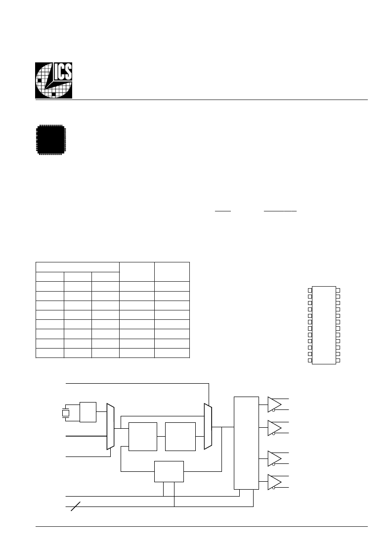
B
LOCK
D
IAGRAM
Pulldown
nPLL_SEL
XTAL_IN
XTAL_OUT
TEST_CLK
nXTAL_SEL
MR
F_SEL0:2
Q0
Q1
nQ1
Q2
nQ2
Q3
nQ3
Pulldown
Pulldown
Pulldown
s
u
L
E
S
0
0
1
1
0
0
1
1
p
n
F
r
e
d
D
u
V
M
e
r
e
d
D
u
V
N
e
2
L
E
0
0
0
0
1
1
1
1
S
_
F
1
_
0
L
E
0
1
0
1
0
1
0
1
S
_
F
8
4
4
2
2
2
2
0
1
2
2
3
3
3
3
4
3
4
8
1
2
4
8
8
F
UNCTION
T
ABLE
The Preliminary Information presented herein represents a product in prototyping or pre-production. The noted characteristics are based on initial
product characterization. Integrated Circuit Systems, Incorporated (ICS) reserves the right to change any circuitry or specifications without notice.
相關(guān)PDF資料 |
PDF描述 |
|---|---|
| ICS843004A02 | CRYSTAL-TO-3.3V LVPECL FREQUENCY SYNTHESIZER |
| ICS843004AG-02 | CRYSTAL-TO-3.3V LVPECL FREQUENCY SYNTHESIZER |
| ICS843004AG-02T | CRYSTAL-TO-3.3V LVPECL FREQUENCY SYNTHESIZER |
| ICS843004AGI-01 | FEMTOCLOCKS-TM CRYSTAL-TO- 3.3V, 2.5V LVPECL FREQUENCY SYNTHESIZER |
| ICS843004AGI-01LF | FEMTOCLOCKS-TM CRYSTAL-TO- 3.3V, 2.5V LVPECL FREQUENCY SYNTHESIZER |
相關(guān)代理商/技術(shù)參數(shù) |
參數(shù)描述 |
|---|---|
| ICS843004-125 | 制造商:IDT 制造商全稱:Integrated Device Technology 功能描述:FemtoClock? Crystal-to-3.3V LVPECL Frequency Synthesizer |
| ICS843004A01 | 制造商:ICS 制造商全稱:ICS 功能描述:FEMTOCLOCKS-TM CRYSTAL-TO- 3.3V LVPECL FREQUENCY SYNTHESIZER |
| ICS843004A02 | 制造商:ICS 制造商全稱:ICS 功能描述:CRYSTAL-TO-3.3V LVPECL FREQUENCY SYNTHESIZER |
| ICS843004AG | 制造商:ICS 制造商全稱:ICS 功能描述:FEMTOCLOCKS⑩ LVCMOS/CRYSTAL-TO- 3.3V LVPECL FREQUENCY SYNTHESIZER |
| ICS843004AG-01 | 制造商:ICS 制造商全稱:ICS 功能描述:FEMTOCLOCKS-TM CRYSTAL-TO- 3.3V LVPECL FREQUENCY SYNTHESIZER |
發(fā)布緊急采購,3分鐘左右您將得到回復(fù)。