- 您現(xiàn)在的位置:買賣IC網(wǎng) > PDF目錄360785 > ICS94203yF-T Programmable System Frequency Generator for PII/III⑩ PDF資料下載
參數(shù)資料
| 型號(hào): | ICS94203yF-T |
| 英文描述: | Programmable System Frequency Generator for PII/III⑩ |
| 中文描述: | 可編程系統(tǒng)頻率發(fā)生器有價(jià)證券/三⑩ |
| 文件頁(yè)數(shù): | 1/18頁(yè) |
| 文件大小: | 183K |
| 代理商: | ICS94203YF-T |
當(dāng)前第1頁(yè)第2頁(yè)第3頁(yè)第4頁(yè)第5頁(yè)第6頁(yè)第7頁(yè)第8頁(yè)第9頁(yè)第10頁(yè)第11頁(yè)第12頁(yè)第13頁(yè)第14頁(yè)第15頁(yè)第16頁(yè)第17頁(yè)第18頁(yè)
Integrated
Circuit
Systems, Inc.
ICS94203
94203 Rev B 02/13/01
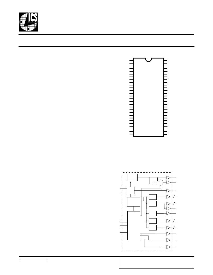
Pin Configuration
Recommended Application:
810/810E and Solano (815) type chipset
Output Features:
2 - CPUs @ 2.5V
13 - SDRAM @ 3.3V
3 - 3V66 @ 3.3V
7 - PCI @3.3V
1 - 24/48MHz@ 3.3V
1 - 48MHz @ 3.3V fixed
1 - REF @3.3V, 14.318MHz
Features:
Programmable ouput frequency
Gear ratio change detection
Real time system reset output
Spread spectrum for EMI control
with programmable spread percentage
Watchdog timer technology to reset system
if over-clocking causes malfunction.
Support power management through PD#.
Uses external 14.318MHz crystal
FS pins for frequency select
Key Specifications:
CPU Output Jitter: <250ps
IOAPIC Output Jitter: <500ps
48MHz, 3V66, PCI Output Jitter: <500ps
CPU Output Skew: <175ps
PCI Output Skew: <500ps
3V66 Output Skew <175ps
For group skew timing, please refer to the
Group Timing Relationship Table.
Programmable System Frequency Generator for P
II
/
III
56-Pin 300 mil SSOP
1. These pins will have 1.5 to 2X drive strength.
* 120K ohm pull-up to VDD on indicated inputs.
VDDA
GNDA
X1
X2
GND3V66
VDD3V66
3V66-0
3V66-1
3V66-2
VDDPCI
GNDPCI
*FS0/PCICLK0
*FS1/PCICLK1
*SEL24_48#/PCICLK2
GNDPCI
VDDPCI
PCICLK3
PCICLK4
PCICLK5
PCICLK6
RATIO_0
PD#
SCLK
SDATA
VDD48
GND48
*FS2/24_48MHz
*FS3/48MHz
1
1
1
REF/FS4*
VDDLAPIC
IOAPIC0
VDDLCPU
GNDLCPU
CPUCLK0
CPUCLK1
GNDSDR
VDDSDR
SDRAM0
SDRAM1
SDRAM2
SDRAM3
VDDSDR
GNDSDR
SDRAM4
SDRAM5
SDRAM6
SDRAM7
SDRAM_F
GNDSDR
VDDSDR
SDRAM8
SDRAM9
SDRAM10
SDRAM11
RESET#
RATIO_1
1
I
1
2
3
4
5
6
7
8
9
10
11
12
13
14
15
16
17
18
19
20
21
22
23
24
25
26
27
28
56
55
54
53
52
51
50
49
48
47
46
45
44
43
42
41
40
39
38
37
36
35
34
33
32
31
30
29
Block Diagram
PLL2
PLL1
Spread
Spectrum
48MHz
24_48MHz
CPUCLK (1:0)
2
12
7
3
SDRAM (11:0)
IOAPIC
PCICLK (6:0)
SDRAM_F
3V66 (2:0)
RESET#
RATIO_0
RATIO_1
X1
X2
XTAL
OSC
CPU
DIVDER
SDRAM
DIVDER
IOAPIC
DIVDER
PCI
DIVDER
3V66
DIVDER
FS(4:0)
PD#
SEL24_48#
SDATA
SCLK
Control
Logic
Config.
Reg.
/ 2
REF
Power Groups
VDDA, GNDA = Core PLL, Xtal
VDD48, GND48 = 48MHz, Fixed PLL
ICS reserves the right to make changes in the device data identified in
this publication without further notice. ICS advises its customers to
obtain the latest version of all device data to verify that any
information being relied upon by the customer is current and accurate.
相關(guān)PDF資料 |
PDF描述 |
|---|---|
| ICS94206 | Programmable System Frequency Generator for PII/III⑩ |
| ICS94206yF-T | Circular Connector; No. of Contacts:10; Series:; Body Material:Aluminum; Connecting Termination:Solder; Connector Shell Size:12; Circular Contact Gender:Pin; Circular Shell Style:Jam Nut Receptacle; Insert Arrangement:12-98 |
| ICS94215YF-T | Programmable System Clock Chip for AMD - K7⑩ Processor |
| ICS94215 | Replaced by SN74ABT16540A : 16-Bit Buffers/Drivers With 3-State Outputs 48-TSSOP -40 to 85 |
| ICS94225 | AMD-K7TM System Clock Chip |
相關(guān)代理商/技術(shù)參數(shù) |
參數(shù)描述 |
|---|---|
| ICS94206 | 制造商:ICS 制造商全稱:ICS 功能描述:Programmable System Frequency Generator for PII/III⑩ |
| ICS94206YF-T | 制造商:ICS 制造商全稱:ICS 功能描述:Programmable System Frequency Generator for PII/III⑩ |
| ICS94209 | 制造商:ICS 制造商全稱:ICS 功能描述:Programmable Frequency Generator & Integrated Buffers for Pentium III Processor |
| ICS94209YF-T | 制造商:ICS 制造商全稱:ICS 功能描述:Programmable Frequency Generator & Integrated Buffers for Pentium III Processor |
| ICS94211 | 制造商:ICS 制造商全稱:ICS 功能描述:Programmable System Frequency Generator for PII/III⑩ |
發(fā)布緊急采購(gòu),3分鐘左右您將得到回復(fù)。