- 您現在的位置:買賣IC網 > PDF目錄358001 > IMT4-7-F (DIODES INC) DUAL PNP SMALL SIGNAL SURFACE MOUNT TRANSISTOR PDF資料下載
參數資料
| 型號: | IMT4-7-F |
| 廠商: | DIODES INC |
| 元件分類: | 小信號晶體管 |
| 英文描述: | DUAL PNP SMALL SIGNAL SURFACE MOUNT TRANSISTOR |
| 中文描述: | 50 mA, 120 V, 2 CHANNEL, PNP, Si, SMALL SIGNAL TRANSISTOR |
| 封裝: | GREEN, PLASTIC PACKAGE-6 |
| 文件頁數: | 1/3頁 |
| 文件大小: | 106K |
| 代理商: | IMT4-7-F |
NOT RECOMMENDED
FOR NEW DESIGN
IMT4
DUAL PNP SMALL SIGNAL SURFACE MOUNT TRANSISTOR
Features
Epitaxial Planar Die Construction
Complementary NPN Type Available (IMX8)
Small Surface Mount Package
Lead Free/RoHS Compliant (Note 3)
"Green" Device, Note 4 and 5
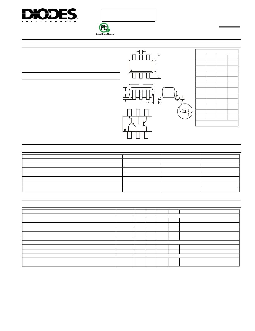
Mechanical Data
Case: SOT-26
Case Material: Molded Plastic, "Green" Molding
Compound, Note 5. UL Flammability Classification
Rating 94V-0
Moisture Sensitivity: Level 1 per J-STD-020C
Terminal Connections: See Diagram
Terminals: Solderable per MIL-STD-202, Method 208
Lead Free Plating (Matte Tin Finish annealed over
Copper leadframe).
Marking Information: KX7 - See Page 3
Ordering & Date Code Information: See Page 3
Weight: 0.016 grams (approximate)
SOT-26
Min
0.35
1.50
2.70
2.90
0.013
1.00
0.35
0.10
0
°
All Dimensions in mm
Dim
A
B
C
D
F
H
J
K
L
M
α
Max
0.50
1.70
3.00
3.10
0.10
1.30
0.55
0.20
8
°
Typ
0.38
1.60
2.80
0.95
0.55
3.00
0.05
1.10
0.40
0.15
Maximum Ratings
@T
A
= 25°C unless otherwise specified
B
2
B
1
E
1
C
2
E
2
C
1
A
M
J
L
D
F
B C
H
K
B
2
B
1
E
1
C
2
E
2
C
1
Characteristic
Symbol
V
CBO
V
CEO
V
EBO
I
C
P
d
R
θ
JA
T
j
, T
STG
Value
-120
-120
-5.0
-50
225
555
-55 to +150
Unit
V
V
V
mA
mW
°
C/W
°
C
Collector-Base Voltage
Collector-Emitter Voltage
Emitter-Base Voltage
Collector Current - Continuous
Power Dissipation (Note 1)
Thermal Resistance, Junction to Ambient (Note 1)
Operating and Storage Temperature Range
Electrical Characteristics
@T
A
= 25°C unless otherwise specified
Characteristic
Symbol
Min
Typ
Max
Unit
Test Condition
OFF CHARACTERISTICS (Note 2)
Collector-Base Breakdown Voltage
Collector-Emitter Breakdown Voltage
Emitter-Base Breakdown Voltage
Collector Cutoff Current
Emitter Cutoff Current
ON CHARACTERISTICS (Note 2)
DC Current Gain
Collector-Emitter Saturation Voltage
SMALL SIGNAL CHARACTERISTICS
V
(BR)CBO
V
(BR)CEO
V
(BR)EBO
I
CBO
I
EBO
-120
-120
-5.0
-0.5
-0.5
V
V
V
μ
A
μ
A
I
C
= -50
μ
A
I
C
= -1.0mA
I
E
= -50
μ
A
V
CB
= -100V
V
EB
= -4.0V
h
FE
180
820
-0.5
V
I
C
= -2.0mA, V
CE
= -6.0V
I
C
= -10mA, I
B
= -1.0mA
V
CE(SAT)
Current Gain-Bandwidth Product
f
T
140
MHz V
CE
= -12V, I
C
= -2.0mA,
f = 100MHz
Notes:
1. Device mounted on FR-5 PCB 1.0 x 0.75 x 0.062 inch pad layout as shown on Diodes Inc. suggested pad layout AP02001, which can be found on our
website at http://www.diodes.com/datasheets/ap02001.pdf. 200mW per element must not be exceeded.
2. Short duration pulse test used to minimize self-heating effect.
3. No purposefully added lead.
4. Diodes Inc.'s "Green" policy can be found on our website at http://www.diodes.com/products/lead_free/index.php.
5. Product manufactured with Date Code 0627 (week 27, 2006) and newer are built with Green Molding Compound. Product manufactured prior to Date
Code 0627 are built with Non-Green Molding Compound and may contain Halogens or Sb2O3 Fire Retardants.
DS30303 Rev. 9 - 3
1 of 3
www.diodes.com
IMT4
Diodes Incorporated
相關PDF資料 |
PDF描述 |
|---|---|
| IMT4 | DUAL PNP SMALL SIGNAL SURFACE MOUNT TRANSISTOR |
| IMT4 | General purpose (dual transistors) |
| IMT5AT109 | 100 mA, 25 V, 2 CHANNEL, PNP, Si, SMALL SIGNAL TRANSISTOR |
| IMX8-7-F | DUAL NPN SMALL SIGNAL SURFACE MOUNT TRANSISTOR |
| IMX8-7 | GT 3C 3#16S PIN PLUG |
相關代理商/技術參數 |
參數描述 |
|---|---|
| IMT4T108 | 功能描述:兩極晶體管 - BJT DUAL PNP 120V 50MA SOT-457 RoHS:否 制造商:STMicroelectronics 配置: 晶體管極性:PNP 集電極—基極電壓 VCBO: 集電極—發射極最大電壓 VCEO:- 40 V 發射極 - 基極電壓 VEBO:- 6 V 集電極—射極飽和電壓: 最大直流電集電極電流: 增益帶寬產品fT: 直流集電極/Base Gain hfe Min:100 A 最大工作溫度: 安裝風格:SMD/SMT 封裝 / 箱體:PowerFLAT 2 x 2 |
| IMT-901 | 制造商:NANOTEC 功能描述:IC STEPPER MOTOR DRIVER SIL-25 制造商:NANOTEC 功能描述:IC, STEPPER MOTOR DRIVER, SIL-25 |
| IM-T-9A | 制造商:Banner Engineering 功能描述:Module; Safety; DIN Rail Mount; Interface 制造商:Banner Engineering 功能描述:INTERFACING MODULE 制造商:Banner Engineering 功能描述:INTERFACING MODULE; Accessory Type:Interface Module; For Use With:Banner Primary Safety Device; Control Output Type:3PST-NO; Supply Voltage Max:24VDC ;RoHS Compliant: Yes |
| IMTA1.66SMVF | 制造商:Banner Engineering 功能描述:FIBER IMTA1.66SFVF |
| IMTAP.753P | 制造商:Banner Engineering 功能描述:Sensor, Glass Fiber Optics, 21074 |
發布緊急采購,3分鐘左右您將得到回復。