- 您現在的位置:買賣IC網 > PDF目錄360924 > IRF054SMD (SEMELAB LTD) N-CHANNEL POWER MOSFET PDF資料下載
參數資料
| 型號: | IRF054SMD |
| 廠商: | SEMELAB LTD |
| 元件分類: | JFETs |
| 英文描述: | N-CHANNEL POWER MOSFET |
| 中文描述: | 45 A, 60 V, 0.031 ohm, N-CHANNEL, Si, POWER, MOSFET |
| 封裝: | HERMETIC SEALED, SMD1, 3 PIN |
| 文件頁數: | 2/2頁 |
| 文件大小: | 22K |
| 代理商: | IRF054SMD |
IRF054SMD
Prelim. 7/00
LA B
S E M E
Semelab plc.
Telephone +44(0)1455 556565. Fax +44(0)1455 552612.
E-mail:
sales@semelab.co.uk
http://www.semelab.co.ukParameter
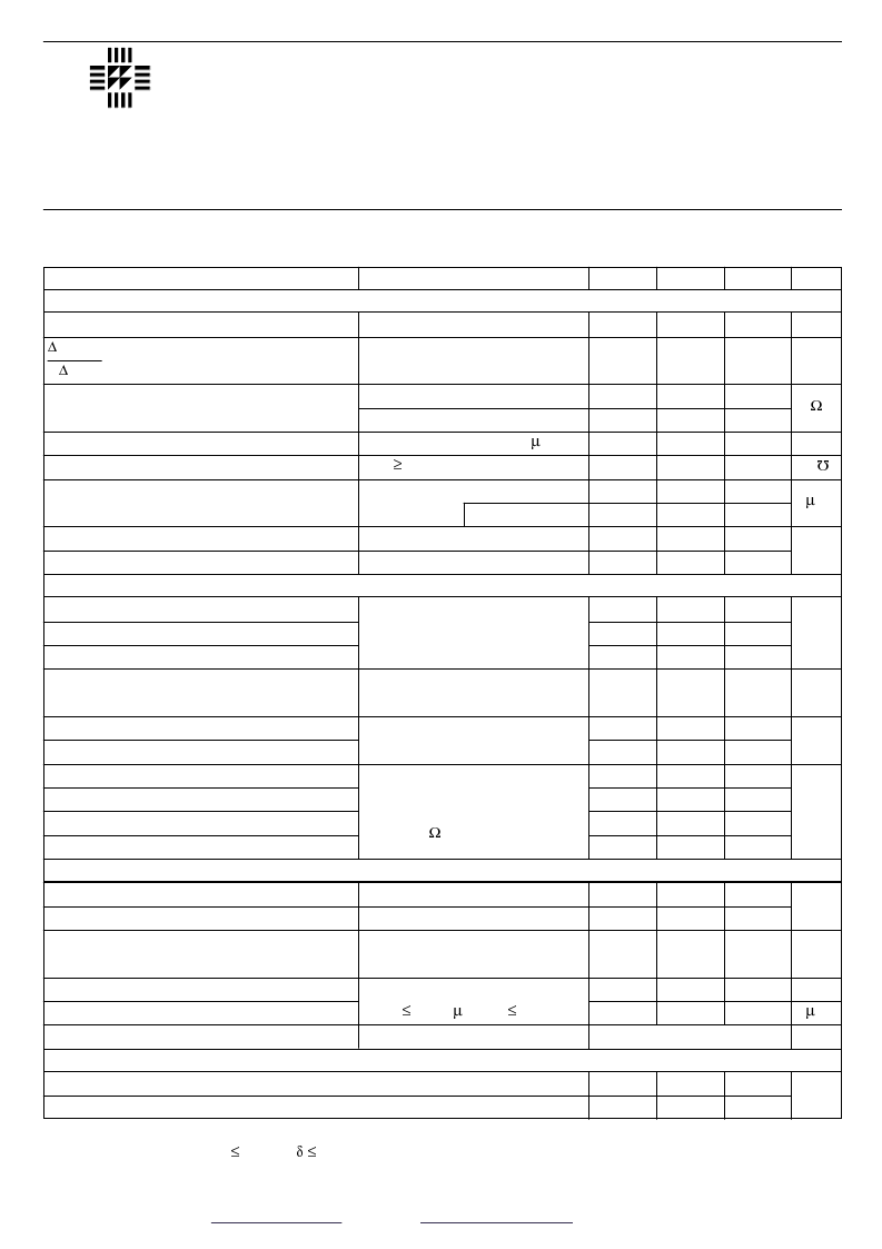
STATIC ELECTRICAL RATINGS
Test Conditions
Min.
Typ.
Max.
Unit
V
GS
= 0
Reference to 25°C
I
D
= 1mA
V
GS
= 10V
V
GS
= 10V
V
DS
= V
GS
V
DS
3
15V
V
GS
= 0
I
D
= 1mA
I
D
= 28A
I
D
= 45A
I
D
= 250
m
A
I
DS
= 28A
V
DS
= 0.8BV
DSS
T
J
= 125°C
V
GS
= 20V
V
GS
= –20V
V
GS
= 0
V
DS
= 25V
f = 1MHz
V
GS
= 10V
V
DS
= 0.5BV
DSS
I
D
= 45A
V
DS
= 0.5BV
DSS
I
D
= 45A
V
DD
= 30V
I
D
= 45A
R
G
= 2.35
W
I
S
= 45A
V
GS
= 0
I
F
= 45A
d
i
/ d
t
£
100A/
m
s V
DD
£
50V
T
J
= 25°C
T
J
= 25°C
ELECTRICAL CHARACTERISTICS
(Tamb= 25°C unless otherwise stated)
Drain – Source Breakdown Voltage
Temperature Coefficient of
Breakdown Voltage
Static Drain – Source On–State
Resistance
1
Gate Threshold Voltage
Forward Transconductance
1
Zero Gate Voltage Drain Current
Forward Gate
– Source Leakage
Reverse Gate
– Source Leakage
Input Capacitance
Output Capacitance
Reverse Transfer Capacitance
Total Gate Charge
1
Gate – Source Charge
1
Gate – Drain (“Miller”) Charge
1
Turn–On Delay Time
Rise Time
Turn–Off Delay Time
Fall Time
Continuous Source Current
Pulse Source Current
2
Diode Forward Voltage
Reverse Recovery Time
Reverse Recovery Charge
Forward Turn–On Time
60
0.68
0.027
0.031
4
2
20
25
250
100
–100
4600
2000
340
80
180
20
34
45
105
33
180
100
100
45
180
2.5
280
2.2
Negligible
0.8
2.8
V
V/°C
W
V
S
(
(
W
)
m
A
nA
pF
nC
nC
ns
A
V
ns
m
C
nH
BV
DSS
D
BV
DSS
D
T
J
R
DS(on)
V
GS(th)
g
fs
I
DSS
I
GSS
I
GSS
C
iss
C
oss
C
rss
Q
g
Q
gs
Q
gd
t
d(on)
t
r
t
d(off)
t
f
I
S
I
SM
V
SD
t
rr
Q
rr
t
on
L
D
L
S
Notes
1) Pulse Test: Pulse Width
£
300ms,
d £
2%
2) Repetitive Rating – Pulse width limited by maximum junction temperature.
DYNAMIC CHARACTERISTICS
SOURCE – DRAIN DIODE CHARACTERISTICS
Internal Drain Inductance
(from centre of drain pad to die)
Internal Source Inductance
(from centre of source pad to end of source bond wire)
PACKAGE CHARACTERISTICS
相關PDF資料 |
PDF描述 |
|---|---|
| IRF1010 | TRANSISTOR | MOSFET | N-CHANNEL | 55V V(BR)DSS | 75A I(D) | TO-220AB |
| IRF1010ESL | |
| IRF1010NSTRL | TRANSISTOR | MOSFET | N-CHANNEL | 55V V(BR)DSS | 84A I(D) | TO-263AB |
| IRF1010NSTRR | TRANSISTOR | MOSFET | N-CHANNEL | 55V V(BR)DSS | 84A I(D) | TO-263AB |
| IRF1010S | TRANSISTOR | MOSFET | N-CHANNEL | 55V V(BR)DSS | 75A I(D) | TO-263AB |
相關代理商/技術參數 |
參數描述 |
|---|---|
| IRF-1 | 制造商:VISHAY 制造商全稱:Vishay Siliconix 功能描述:Inductors Epoxy Conformal Coated Uniform Roll Coated |
| IRF100 | 制造商:未知廠家 制造商全稱:未知廠家 功能描述:50W to 500W HIGH POWER WIRE WOUND RESISTORS FLAT SHAPED ALUMINUM HOUSED |
| IRF100S | 制造商:未知廠家 制造商全稱:未知廠家 功能描述:Analog IC |
發布緊急采購,3分鐘左右您將得到回復。