- 您現在的位置:買賣IC網 > Datasheet目錄38 > IRS2500SPBF (International Rectifier)IC PFC Datasheet資料下載
參數資料
| 型號: | IRS2500SPBF |
| 廠商: | International Rectifier |
| 文件頁數: | 13/22頁 |
| 文件大小: | 419K |
| 描述: | IC PFC |
| 產品培訓模塊: | IRS2500 PFC Control IC Overview |
| 標準包裝: | 95 |
| 系列: | * |
IRS2500S
www.irf.com
?2012 International Rectifier
13
level and the discharge time will be longer giving a
lower switching frequency.
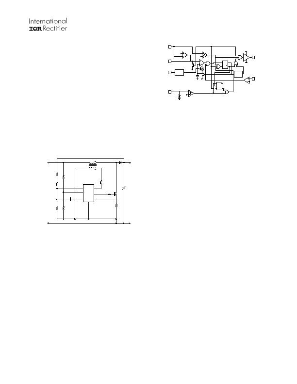
The PFC control circuit of the IRS2500 (Figure
10) includes six control pins: VBUS, COMP, ZX,
OUT, VDC and OC. The VBUS pin measures the
DC bus voltage through an external resistor voltage
divider. The COMP pin voltage determines the on-
time of MPFC and sets the feedback loop response
speed with an external RC integrator. The ZX pin
detects when the inductor current discharges to
zero each switching cycle using a secondary
winding from the PFC inductor. The OUT pin is the
low-side gate driver output for the external
MOSFET, MPFC. The VDC pin senses the line
input cycle providing phase information to control
the on time modulation described in the next
section. The OC pin senses the current flowing
through MPFC and performs cycle-by-cycle over-
current protection.
RVBUS1
RVBUS2
RVBUS
CCOMP
LPFC
MPFC
RPFC
DFPC
CBUS
(+)
(-)
RZX
PFC
Control
VBUS
COMP
OUT
ZX
COM
OC
ROC
RDC
RIN
VDC
Figure 10: IRS2500 simplified PFC control
circuit.
The VBUS pin is compared with a fixed internal
2.5V reference voltage for regulating the DC output
voltage (Figure 11). The feedback loop error
amplifier increases or decreases the COMP pin
voltage. The resulting voltage on the COMP pin
sets the threshold for the charging of the internal
timing capacitor (C1, Figure 11) and therefore
determines the on-time of MPFC.
The error amplifier operates at a slow loop speed
preventing rapid changes in PWM duty cycle during
a single input line cycle. This prevents distortion
achieving high power factor and low THD.
5
2
1
Q
S
R Q
2.0V
VBUS
COMP
ZX
5.1V
2.5V
2.75
7
OUT
Q
S
R2 Q
R1
COMP3
COMP4
COMP5
RS3
RS4
VCC
M1
WATCH
DOG
TIMER
M2
C1
4
OC
1.2V
On Time
Modulator
3
VDC
Figure 11: IRS2500 detailed PFC control circuit.
The off-time of MPFC is determined by the time it
takes the LPFC current to discharge to zero. The
zero current level is detected by a secondary
winding on LPFC that is connected to the ZX pin
through an external current limiting resistor RZX. A
positive-going edge exceeding the internal
threshold VZX+ signals the beginning of the off-
time. A negative-going edge on the ZX pin falling
below VZX- will occur when the LPFC current
discharges to zero, which signals the end of the off-
time and MPFC is turned on again (Figure 12). The
ZX pin is internally biased to ensure that the voltage
detected from the inductor drops fully to zero before
triggering the next PWM cycle. A wide hysteresis
prevents false triggering by ringing oscillations.
The cycle repeats itself indefinitely until the
IRS2500 is disabled through an over-voltage
condition on the DC bus or if the negative transition
of ZX pin voltage does not occur. Should the
negative edge on the ZX pin not occur, MPFC will
remain off until the watch-dog timer forces a turn-on
of MPFC for an on-time duration programmed by
the voltage on the COMP pin. The watch-dog
pulses occur every 300-400us (tWD) indefinitely
until a correct positive and negative-going signal is
detected at the ZX pin and normal operation is
resumed. Should the OC pin voltage exceed the
VOCTH over-current threshold during the on-time
the gate drive output will turn off. The circuit will
then wait for a negative-going transition on the ZX
pin or a forced turn-on from the watch-dog timer to
turn the output on again.
相關PDF資料 |
PDF描述 |
|---|---|
| IRS2548DSPBF | IC PFC |
| IRS2580DSPBF | IC PFC |
| ISL6111CR-T | IC CTRLR HOT PLUG SWITCH 20-QFN |
| ISL6112INZA-T | IC PWR CNTRLR DUAL SLT 48-TQFP |
| ISL6114IRZA | IC HOT PLUG CTRLR PCI-E 48-QFN |
相關代理商/技術參數 |
參數描述 |
|---|---|
| IRS2500STRPBF | 功能描述:功率因數校正 IC PFC controller IC RoHS:否 制造商:Fairchild Semiconductor 開關頻率:300 KHz 最大功率耗散: 最大工作溫度:+ 125 C 安裝風格:SMD/SMT 封裝 / 箱體:SOIC-8 封裝:Reel |
| IRS2500STRPBF-CUT TAPE | 制造商:IR 功能描述:IRS2500 Series Fully Integrated Fully Protected PFC SMPS Control IC - SOIC-8 |
| IRS2505LPBF | 制造商:IRF 制造商全稱:International Rectifier 功能描述:SOT-23 Boost PFC Control IC |
| IRS2505LTRPBF | 制造商:International Rectifier 功能描述:PFC BOOST IC - Tape and Reel 制造商:International Rectifier 功能描述:IC PFC MOSFET SOT-23-5 制造商:International Rectifier 功能描述:IRS2505 Series 14 V 10 mA 20.8 VCLAMP 250 mW Boost PFC Control IC - SOT-23-5 制造商:International Rectifier 功能描述:Power Factor Correction - PFC CTRL IC Boost PFC 20.8V VCC 25mA 250mW 制造商:International Rectifier 功能描述:T&R / PFC Boost IC |
| IRS25091SPBF | 功能描述:功率驅動器IC Half-Bridge Driver 600V 10V to 20V RoHS:否 制造商:Micrel 產品:MOSFET Gate Drivers 類型:Low Cost High or Low Side MOSFET Driver 上升時間: 下降時間: 電源電壓-最大:30 V 電源電壓-最小:2.75 V 電源電流: 最大功率耗散: 最大工作溫度:+ 85 C 安裝風格:SMD/SMT 封裝 / 箱體:SOIC-8 封裝:Tube |
發布緊急采購,3分鐘左右您將得到回復。