- 您現在的位置:買賣IC網 > PDF目錄67723 > ISL8703IBZT (INTERSIL CORP) DSP-ADDRESS SEQUENCER, PDSO14 PDF資料下載
參數資料
| 型號: | ISL8703IBZT |
| 廠商: | INTERSIL CORP |
| 元件分類: | 數字信號處理外設 |
| 英文描述: | DSP-ADDRESS SEQUENCER, PDSO14 |
| 封裝: | PLASTIC, MS-012AB, SOIC-14 |
| 文件頁數: | 1/12頁 |
| 文件大小: | 351K |
| 代理商: | ISL8703IBZT |
1
FN9250.0
CAUTION: These devices are sensitive to electrostatic discharge; follow proper IC Handling Procedures.
1-888-INTERSIL or 1-888-468-3774
| Intersil (and design) is a registered trademark of Intersil Americas Inc.
Copyright Intersil Americas Inc. 2006. All Rights Reserved
All other trademarks mentioned are the property of their respective owners.
ISL8700, ISL8701, ISL8702, ISL8702A,
ISL8703, ISL8704, ISL8705
Adjustable Quad Sequencer
The ISL8700, ISL8701, ISL8702, ISL8702A, ISL8703,
ISL8704, ISL8705 family of ICs provide four delay adjustable
sequenced outputs while monitoring an input voltage all with
a minimum of external components.
High performance DSP, FPGA, P and various subsystems
require input power sequencing for proper functionality at
initial power up and the ISL870X provides this function while
monitoring the distributed voltage for over and undervoltage
compliance.
The ISL8700 and ISL8701 operate over the +2.5V to +24V
nominal voltage range, whereas the ISL8702 operates over
the 2.5V to +12V range. All three have a user adjustable
time from UV and OV voltage compliance to sequencing
start via an external capacitor when in auto start mode and
adjustable time delay to subsequent ENABLE output signal
via external resistors.
Additionally, ISL8702A, ISL8703, ISL8704 and ISL8705
provide I/O for sequencing on and off operation (SEQ_EN)
and for voltage window compliance reporting (FAULT) over
the +2.5V to +24V voltage range. The ISL8702 also has this
feature but operates over the 2.5V to +12V range.
Easily daisy chained for more than 4 sequenced signals.
Altogether, the ISL870X provides these adjustable features
with a minimum of external BOM. See Figure 1 for typical
implementation.
Features
Adjustable Delay to Subsequent Enable Signal
Adjustable Delay to Sequence Auto Start
Adjustable Distributed Voltage Monitoring
Under and Overvoltage Adjustable Delay to Auto Start
Sequence
I/O Options
ENABLE (ISL8700, ISL8702, ISL8702A, ISL8704) and
ENABLE# (ISL8701, ISL8703, ISL8705)
SEQ_EN (ISL8702, ISL8702A, ISL8703) and SEQ_EN#
(ISL8704, ISL8705)
Voltage Compliance Fault Output
Pb-Free Plus Anneal Available (RoHS Compliant)
Applications
Power Supply Sequencing
System Timing Function
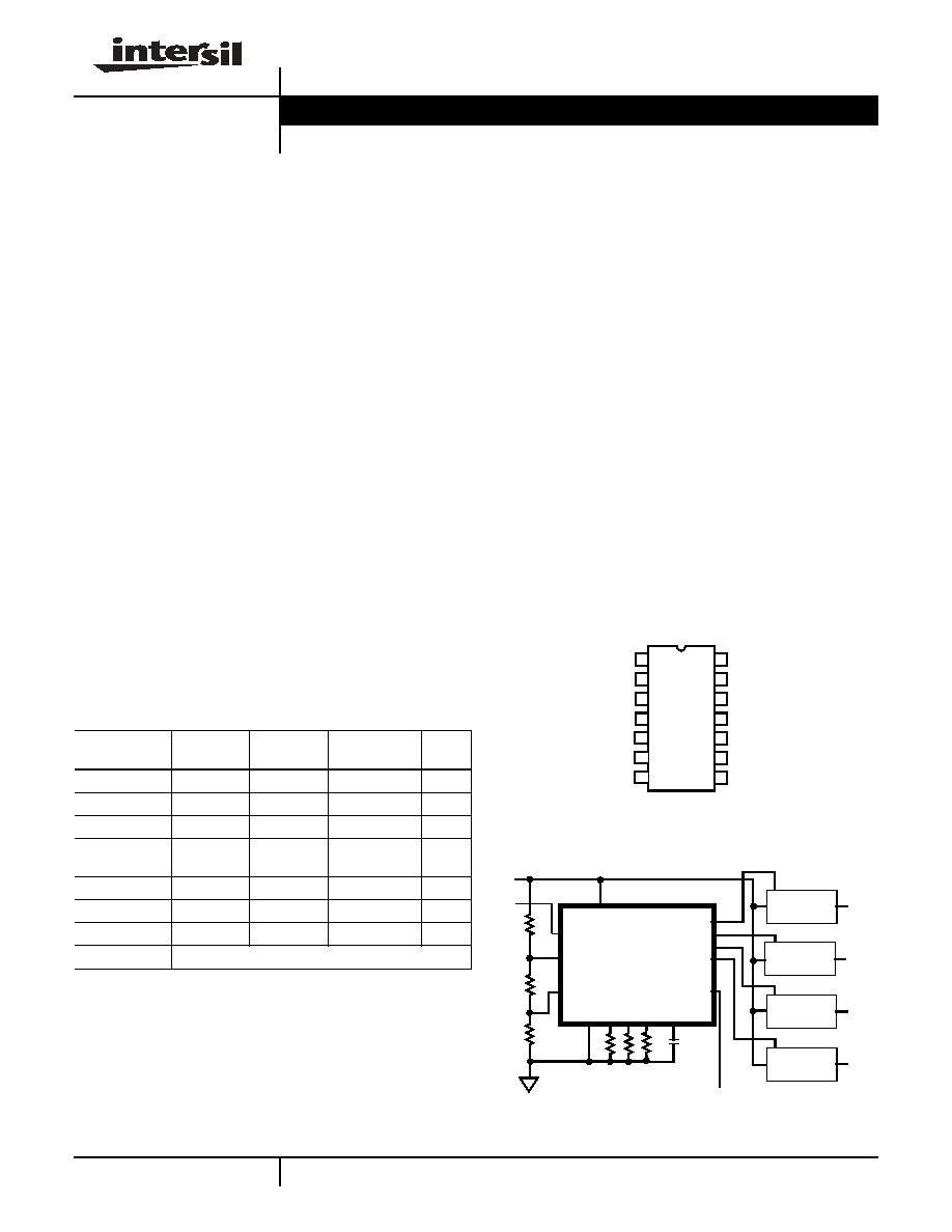
Pinout
ISL870X
(14 LD SOIC)
TOP VIEW
Ordering Information
PART NUMBER
(Notes 1, 2)
PART
MARKING
TEMP.
RANGE (°C)
PACKAGE
(Pb-free)
PKG.
DWG. #
ISL8700IBZ*
ISL8700IBZ
-40 to +85 14 Ld SOIC
M14.15
ISL8701IBZ*
ISL8701IBZ
-40 to +85 14 Ld SOIC
M14.15
ISL8702IBZ*
ISL8702IBZ
-40 to +85 14 Ld SOIC
M14.15
ISL8702AIBZ-T
-40 to +85 14 Ld SOIC
(Tape and Reel)
M14.15
ISL8703IBZ*
ISL8703IBZ
-40 to +85 14 Ld SOIC
M14.15
ISL8704IBZ*
ISL8704IBZ
-40 to +85 14 Ld SOIC
M14.15
ISL8705IBZ*
ISL8705IBZ
-40 to +85 14 Ld SOIC
M14.15
ISL870XEVAL1 Evaluation Platform
*Add “-T” suffix for tape and reel.
NOTES:
1. Part Numbers in Bold are available now, others will soon be available,
contact factory for availability schedule.
2. Intersil Pb-free plus anneal products employ special Pb-free material
sets; molding compounds/die attach materials and 100% matte tin
plate termination finish, which are RoHS compliant and compatible with
both SnPb and Pb-free soldering operations. Intersil Pb-free products
are MSL classified at Pb-free peak reflow temperatures that meet or
exceed the Pb-free requirements of IPC/JEDEC J STD-020.
ENABLE_D
ENABLE_C
ENABLE_B
ENABLE_A
1
2
3
4
5
VIN
TD
TC
TB
6
7
8
9
14
TIME
SEQ_EN (NC on ISL8700/01)
FAULT (NC on ISL8700/01)
OV
UV
GND
13
12
11
10
ISL8701, ISL8703, ISL8705 PINS 1-4 ARE ENABLE# FUNCTION
ISL8704, ISL8705 PIN 9 IS SEQ_EN# FUNCTION
ENABLE_A
UV
OV
GND TB TC TD TIME
VIN
FAULT *
SEQ_EN *
ENABLE_B
ENABLE_C
ENABLE_D
2.5-24V (12Vmax for ISL8702)
DC/DC
EN
DC/DC
EN
DC/DC
EN
DC/DC
EN
Vo1
Vo2
Vo3
V04
FIGURE 1. ISL870X IMPLEMENTATION
* SEQ_EN and FAULT are not available on ISL8700 and ISL8701
Ru
Rm
Rl
Data Sheet
March 14, 2006
相關PDF資料 |
PDF描述 |
|---|---|
| ISP1160BD-S | UNIVERSAL SERIAL BUS CONTROLLER, PQFP64 |
| ISP1160BD/01,118 | UNIVERSAL SERIAL BUS CONTROLLER, PQFP64 |
| ISP1160BD/01,151 | UNIVERSAL SERIAL BUS CONTROLLER, PQFP64 |
| ISP1161A1BM,557 | UNIVERSAL SERIAL BUS CONTROLLER, PQFP64 |
| ISP1181BBS,551 | UNIVERSAL SERIAL BUS CONTROLLER, PQCC48 |
相關代理商/技術參數 |
參數描述 |
|---|---|
| ISL8704AIBZ | 功能描述:監控電路 ADJ QD SEQNCR 14N W/ANNEAL RoHS:否 制造商:STMicroelectronics 監測電壓數: 監測電壓: 欠電壓閾值: 過電壓閾值: 輸出類型:Active Low, Open Drain 人工復位:Resettable 監視器:No Watchdog 電池備用開關:No Backup 上電復位延遲(典型值):10 s 電源電壓-最大:5.5 V 最大工作溫度:+ 85 C 安裝風格:SMD/SMT 封裝 / 箱體:UDFN-6 封裝:Reel |
| ISL8704AIBZ-T | 功能描述:監控電路 ADJ QD SEQNCR 14N W/ANNEAL RoHS:否 制造商:STMicroelectronics 監測電壓數: 監測電壓: 欠電壓閾值: 過電壓閾值: 輸出類型:Active Low, Open Drain 人工復位:Resettable 監視器:No Watchdog 電池備用開關:No Backup 上電復位延遲(典型值):10 s 電源電壓-最大:5.5 V 最大工作溫度:+ 85 C 安裝風格:SMD/SMT 封裝 / 箱體:UDFN-6 封裝:Reel |
| ISL8705AIBZ | 功能描述:監控電路 ADJ QD SEQNCR 14N W/ANNEAL RoHS:否 制造商:STMicroelectronics 監測電壓數: 監測電壓: 欠電壓閾值: 過電壓閾值: 輸出類型:Active Low, Open Drain 人工復位:Resettable 監視器:No Watchdog 電池備用開關:No Backup 上電復位延遲(典型值):10 s 電源電壓-最大:5.5 V 最大工作溫度:+ 85 C 安裝風格:SMD/SMT 封裝 / 箱體:UDFN-6 封裝:Reel |
| ISL8705AIBZ-T | 功能描述:監控電路 ADJ QD SEQNCR 14N W/ANNEAL RoHS:否 制造商:STMicroelectronics 監測電壓數: 監測電壓: 欠電壓閾值: 過電壓閾值: 輸出類型:Active Low, Open Drain 人工復位:Resettable 監視器:No Watchdog 電池備用開關:No Backup 上電復位延遲(典型值):10 s 電源電壓-最大:5.5 V 最大工作溫度:+ 85 C 安裝風格:SMD/SMT 封裝 / 箱體:UDFN-6 封裝:Reel |
| ISL870XEVAL1 | 功能描述:EVAL BOARD 1 FOR ISL870X RoHS:否 類別:編程器,開發系統 >> 評估演示板和套件 系列:* 標準包裝:1 系列:PSoC® 主要目的:電源管理,熱管理 嵌入式:- 已用 IC / 零件:- 主要屬性:- 次要屬性:- 已供物品:板,CD,電源 |
發布緊急采購,3分鐘左右您將得到回復。