- 您現(xiàn)在的位置:買賣IC網(wǎng) > PDF目錄360996 > ISO102 SIGNAL ISOLATION BUFFER AMPLIFIERS PDF資料下載
參數(shù)資料
| 型號: | ISO102 |
| 英文描述: | SIGNAL ISOLATION BUFFER AMPLIFIERS |
| 中文描述: | 信號隔離緩沖放大器 |
| 文件頁數(shù): | 4/15頁 |
| 文件大小: | 230K |
| 代理商: | ISO102 |
4
ISO102/106
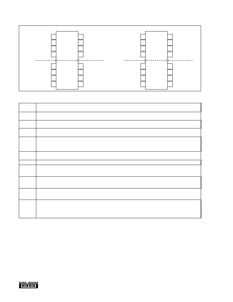
PIN CONFIGURATION
–V
V
Gain Adjust
Common
C
Common
Reference
+V
+V
Offset Adjust
Offset
Reference
Digital Common
C
V
–V
1
2
3
4
9
10
11
12
24
23
22
21
16
15
14
13
CC1
ISO102
1
OUT
CC2
2
Isolation
Barrier
1
1
2
2
–V
V
IN
Gain Adjust
Common
C
Common
Reference
+V
+V
Offset Adjust
Offset
Reference
Digital Common
C
V
–V
1
2
3
4
17
18
19
20
40
39
38
37
24
23
22
21
CC1
ISO106
1
OUT
CC2
2
Isolation
Barrier
1
1
2
2
PIN DESCRIPTIONS
±
V
,
Common
1
Positive and negative power supply voltages and common (or ground) for the input stage. Common
is the analog reference voltage for input
signals. The voltage between Common
1
and Common
2
is the isolation voltage and appears across the internal high voltage barrier.
±
V
,
Common
2
Positive and negative power supply voltages and common (or ground) for the output stage. Common
is the analog reference voltage for output
signals. The voltage between Common
1
and Common
2
is the isolation voltage and appears across the internal high voltage barrier.
V
IN
Signal input pin. Input impedance is typically 100k
. The input range is rated for
±
10V. The input level can actually exceed the input stage
supplies. Output signal swing is limited only by the output supply voltages.
Gain
Adjust
This pin is an optional signal input. A series 5k
potentiometer between this pin and the input signal allows a guaranteed
±
1.5% gain adjustment
range. When gain adjustment is not required, the Gain Adjust should be left open. Figure 4 illustrates the gain adjustment connection.
Reference
1
+5V reference output. This low-drift zener voltage reference is necessary for setting the bipolar offset point of the input stage.
This pin must
be strapped to either Offset or Offset Adjust to allow the isolation amplifier to function.
The reference is often useful for input signal
conditioning circuits. See “Effect of Reference Loading on Offset” performance curve for the effect of offset voltage change with reference loading.
Reference
1
is identical to, but independent of, Reference
2
. This output is short circuit protected.
Reference
2
+5V reference output. This reference circuit is identical to, but independent of, Reference
1
. It controls the bipolar offset of the output stage through
an internal connection. This output is short-circuit protected.
Offset
Offset input.
This input must be strapped to Reference
1
unless user adjustment of bipolar offset is required.
Offset
Adjust
This pin is for optional offset control. When connected to the Reference
pin through a 1k
potentiometer,
±
150mV of adjustment range is
guaranteed. Under this condition, the Offset pin should be connected to the Offset Adjust pin. When offset adjustment is not required, the Offset
Adjust pin is left open. See Figure 4.
Digital
Common
Digital common or ground. This separate ground carries currents from the digital portions of the output stage circuit. The best grounding practi-
ces require that digital common current does not flow in analog common connections. Both pins can be tied directly to a ground plane if available.
Difference in potentials between the Common
2
and Digital Common pins can be
±
1V. See Figure 2.
V
OUT
Signal output. Because the isolation amplifier has unity gain, the output signal is ideally identical to the input signal. The output is low impedance
and is short-circuit protected. This signal is referenced to Common
2
; subsequent circuitry should have a separate “sense” connection to Common
1
as well as V
OUT
.
C
1
, C
2
Capacitors for small signal bandwidth control. These pins connect to the internal rolloff frequency controlling nodes of the output low-pass filter.
Additional capacitance added to these pins will modify the bandwidth of the buffer. C
is always twice the value of C
. See “Bandwidth Control”
performance curve for the relationship between bandwidth and C
and C
. When no connections are made to these pins, the full small-signal
bandwidth is maintained. Be sure to shield C
1
and C
2
pins from high electric fields on the PC board. This preserves AC isolation-mode rejection
by reducing capacitive coupling effects.
相關(guān)PDF資料 |
PDF描述 |
|---|---|
| ISO103 | Low-Cost, Internally Powered ISOLATION AMPLIFIER |
| ISO103B | Low-Cost, Internally Powered ISOLATION AMPLIFIER |
| ISO107 | High-Voltage, Internally Powered ISOLATION AMPLIFIER |
| ISO121 | Precision Low Cost ISOLATION AMPLIFIER |
| ISO121BG | Precision Low Cost ISOLATION AMPLIFIER |
相關(guān)代理商/技術(shù)參數(shù) |
參數(shù)描述 |
|---|---|
| ISO102/ISO106 | 制造商:BB 制造商全稱:BB 功能描述:ISO102. ISO106 - SIGNAL ISOLATION BUFFER AMPLIFIERS |
| ISO102B | 功能描述:隔離放大器 Wide BW Std Herm Sig Iso Buffer Amp RoHS:否 制造商:Texas Instruments 輸入補(bǔ)償電壓:1.5 mV 共模抑制比(最小值):95 dB 帶寬:60 KHz 工作電源電壓:3.3 V 電源電流:8 mA 工作溫度范圍:- 40 C to + 105 C 安裝風(fēng)格:SMD/SMT 封裝 / 箱體:SOP-8 封裝:Tube |
| ISO103 | 功能描述:特殊用途放大器 Low-Cost Internally Pwrd Iso Amp RoHS:否 制造商:Texas Instruments 通道數(shù)量:Single 共模抑制比(最小值): 輸入補(bǔ)償電壓: 工作電源電壓:3 V to 5.5 V 電源電流:5 mA 最大功率耗散: 最大工作溫度:+ 70 C 最小工作溫度:- 40 C 安裝風(fēng)格:SMD/SMT 封裝 / 箱體:QFN-20 封裝:Reel |
| ISO103 | 制造商:Texas Instruments 功能描述:IC AMP ISOLATION DIP24 103 |
| ISO103B | 功能描述:特殊用途放大器 Low-Cost Internally Pwrd Iso Amp RoHS:否 制造商:Texas Instruments 通道數(shù)量:Single 共模抑制比(最小值): 輸入補(bǔ)償電壓: 工作電源電壓:3 V to 5.5 V 電源電流:5 mA 最大功率耗散: 最大工作溫度:+ 70 C 最小工作溫度:- 40 C 安裝風(fēng)格:SMD/SMT 封裝 / 箱體:QFN-20 封裝:Reel |
發(fā)布緊急采購,3分鐘左右您將得到回復(fù)。