- 您現在的位置:買賣IC網 > PDF目錄360996 > ISO103 Low-Cost, Internally Powered ISOLATION AMPLIFIER PDF資料下載
參數資料
| 型號: | ISO103 |
| 元件分類: | 隔離放大器 |
| 英文描述: | Low-Cost, Internally Powered ISOLATION AMPLIFIER |
| 中文描述: | 低成本,內部隔離放大器技術 |
| 文件頁數: | 7/9頁 |
| 文件大小: | 112K |
| 代理商: | ISO103 |
7
ISO103
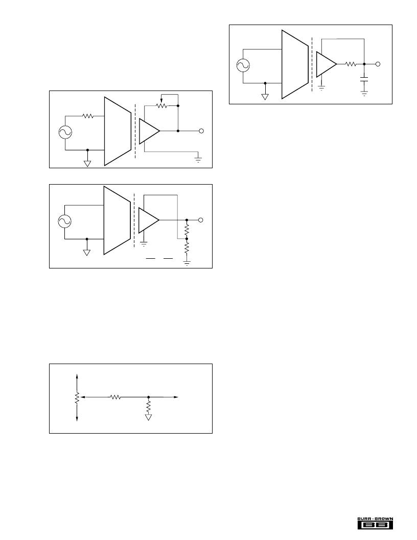
Gains greater than 1 may be obtained by using the circuit of
Figure 2b. Note that the effect of input referred errors will be
multiplied at the output in proportion to the increase in gain.
Also, the small-signal bandwidth will be decreased in in-
verse proportion to the increase in gain. In most instances, a
precision gain block at the input of the isolation amplifier
will provide better overall performance.
FIGURE 2a. Gain Adjust.
FIGURE 2b. Gain Setting.
R
1
V
IN
22
21
R
2
11
9
10
V
OUT
Sense
Gain = 1 +
( )
R
+
R
1
R
1
200k
1k
R
1
V
IN
22
21
2k
R
2
11
9
10
V
OUT
Figure 3 shows a method for trimming V
OS
of the ISO103.
This circuit may be applied to either Signal Com (input or
output) as desired for safety or convenience. With the values
shown,
±
15V supplies and unity gain, the circuit will pro-
vide
±
150mV adjustment range and 0.25mV resolution with
a typical trim potentiometer. The output will have some
sensitivity to power supply variations. For a
±
100mV trim,
power supply sensitivity is 8mV/V at the output.
FIGURE 3. V
OS
Adjust.
Signal Com 1
or
Signal Com 2
1M
100k
10k
+V
CC1
or +V
CC2
–V
CC1
or –V
CC2
OPTIONAL OUTPUT FILTER
Figure 4 shows an optional output ripple filter that reduces
the 800kHz ripple voltage to <5mVp-p without compromis-
ing DC performance. The small signal bandwidth is ex-
tended above 30kHz as a result of this compensation.
FIGURE 4. Ripple Reduction.
V
IN
22
21
11
9
10
V
OUT
Sense
400
4.7nF
MULTICHANNEL SYNCHRONIZATION
Synchronization of multiple ISO103s can be accomplished
by connecting pin 15 of each device to an external TTL level
oscillator, as shown in Figure 7. The PWS750-1 oscillator is
convenient because its nominal synchronizing output fre-
quency is 1.6MHz, resulting in a 800kHz carrier in the
ISO103 (its nominal unsynchronized value). The open col-
lector output typically switches 7.5mA to a 0.2V low level
so that the external pull-up resistor can be chosen for
different pull-up voltages as shown in Figure 7. The number
of channels synchronized by one PWS750-1 is determined
by the total capacitance of the sync voltage conductors. They
must be less than 1000pF to ensure TTL level switching at
800kHz. At higher frequencies the capacitance must be
proportionally lower.
Customers can supply their own TTL level synchronization
logic provided the frequency is between 1.2MHz and 2MHz,
and the duty cycle is greater than 25%.
Multichannel synchronization with reduced power dissipa-
tion for applications requiring less than
±
15mA from V
CC1
is accomplished by driving both the Sync input pin (15) and
Enable pin (13) with the TTL oscillator as shown in Figure 5.
ISOLATION BARRIER VOLTAGE
The typical performance of the ISO103 under conditions of
barrier voltage stress is indicated in the first two perform-
ance curves—Recommended Range of Isolation Voltage
and IMR/ Leakage vs Frequency. At low barrier modulation
levels, errors can be determined by the IMRR characteristic.
At higher barrier voltages, typical performance is obtained
as long as the dv/dt across the barrier is below the shaded
area in the first curve. Otherwise, the signal channel will be
interrupted, causing the output to distort, and/or shift DC
level. This condition is temporary, with normal operation
resuming as soon as the transient subsides. Permanent dam-
age to the integrated circuits occurs only if transients exceed
20kV/
μ
s. Even in this extreme case, the barrier integrity is
assured.
HIGH VOLTAGE TESTING
The ISO103 was designed to reliably operate with 1500Vrms
continuous isolation barrier voltage. To confirm barrier
integrity, a two-step breakdown test is performed on 100%
of the units. First, a 5600V peak, 60Hz barrier potential is
相關PDF資料 |
PDF描述 |
|---|---|
| ISO103B | Low-Cost, Internally Powered ISOLATION AMPLIFIER |
| ISO107 | High-Voltage, Internally Powered ISOLATION AMPLIFIER |
| ISO121 | Precision Low Cost ISOLATION AMPLIFIER |
| ISO121BG | Precision Low Cost ISOLATION AMPLIFIER |
| ISO121G | Precision Low Cost ISOLATION AMPLIFIER |
相關代理商/技術參數 |
參數描述 |
|---|---|
| ISO103 | 制造商:Texas Instruments 功能描述:IC AMP ISOLATION DIP24 103 |
| ISO103B | 功能描述:特殊用途放大器 Low-Cost Internally Pwrd Iso Amp RoHS:否 制造商:Texas Instruments 通道數量:Single 共模抑制比(最小值): 輸入補償電壓: 工作電源電壓:3 V to 5.5 V 電源電流:5 mA 最大功率耗散: 最大工作溫度:+ 70 C 最小工作溫度:- 40 C 安裝風格:SMD/SMT 封裝 / 箱體:QFN-20 封裝:Reel |
| ISO1050 | 制造商:TI 制造商全稱:Texas Instruments 功能描述:ISOLATED CAN TRANSCEIVER |
| ISO1050_10 | 制造商:TI 制造商全稱:Texas Instruments 功能描述:ISOLATED CAN TRANSCEIVER |
| ISO1050_101 | 制造商:TI 制造商全稱:Texas Instruments 功能描述:ISOLATED CAN TRANSCEIVER |
發布緊急采購,3分鐘左右您將得到回復。