- 您現(xiàn)在的位置:買賣IC網(wǎng) > PDF目錄360996 > ISO103B Low-Cost, Internally Powered ISOLATION AMPLIFIER PDF資料下載
參數(shù)資料
| 型號: | ISO103B |
| 元件分類: | 隔離放大器 |
| 英文描述: | Low-Cost, Internally Powered ISOLATION AMPLIFIER |
| 中文描述: | 低成本,內(nèi)部隔離放大器技術(shù) |
| 文件頁數(shù): | 6/9頁 |
| 文件大小: | 112K |
| 代理商: | ISO103B |
ISO103
6
THEORY OF OPERATION
The block diagram on the front page shows the isolation
amplifier’s synchronized signal and power configuration,
which eliminate beat frequency interference. A proprietary
800kHz oscillator chip, power MOSFET transformer driv-
ers, patented square core wirebonded transformer, and single
chip diode bridge provide power to the input side of the
isolation amplifier as well as external loads. The signal
channel capacitively couples a duty-cycle encoded signal
across the ceramic high-voltage barrier built into the pack-
age. A proprietary transmitter-receiver pair of integrated
circuits, laser trimmed at wafer level, and coupled through a
pair of matched “fringe” capacitors, result in a simple,
reliable design.
The ISO103 isolation amplifier contains a transformer-
coupled DC/DC converter that is powered from the output
side of the isolation amplifier. All power supply pins (1, 2,
3, 4, 14, and 16) of the ISO103 have an internal 0.1
μ
F
capacitor to ground. L
1
is used to slow down fast changes in
the input current to the DC/DC converter. C
1
is used to help
regulate the voltage ripple caused by the current demands of
the converter. L
1
, C
1
, and C
2
are optional, however, recom-
mended for low noise applications.
The DC/DC converter creates an unregulated
±
15V output
to
±
V
CC1
. If the ISO103 is the only device using the DC/DC
converter for power, pins 1 and 2 and pins 3 and 4 can be
connected directly without C
O
or L
O
in the circuit. If an
external capacitor is used in this configuration, it should not
exceed 1
μ
F. This configuration is possible because the
isolation amplifier and the DC/DC converter are synchro-
nized internally.
If additional devices are powered by the DC/DC converter
of the ISO103, the application may require that the ripple
voltage of the ISO103 converter be attenuated. In which
case, L
O
and C
O
should be added to the circuit. The inductor
is used to attenuate the ripple current and a higher value
capacitor can be used to reduce the ripple voltage even
further.
OPTIONAL GAIN AND OFFSET ADJUSTMENTS
Rated gain accuracy and offset performance can be achieved
with no external adjustments, but the circuit of Figure 2a
may be used to provide a gain trim of
±
0.5% for the values
shown; greater range may be provided by increasing the size
of R
1
and R
2
. Every 2k
increase in R
1
will give an
additional 1% adjustment range, with R
2
≥
2R
1
. If safety or
convenience dictate location of the adjustment potentiome-
ter on the other side of the barrier from the position shown
in Figure 2a, the position of R
1
and R
2
may be reversed.
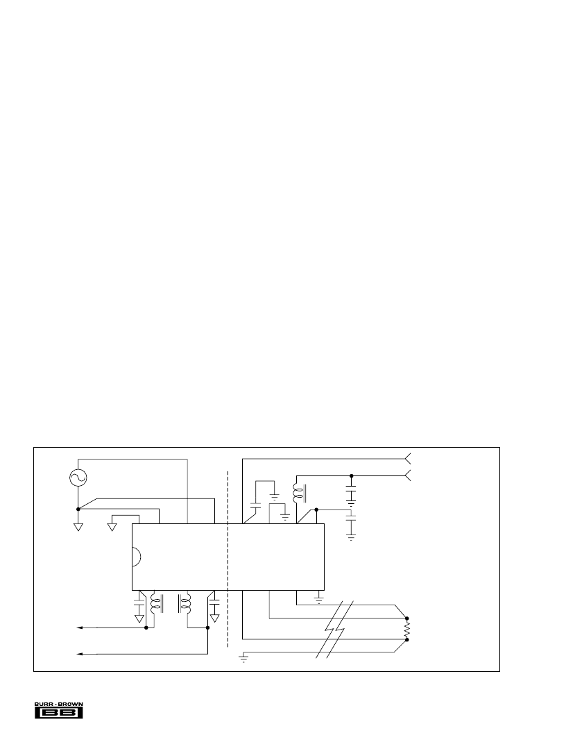
SIGNAL AND POWER CONNECTIONS
Figure 1 shows the proper power supply and signal connec-
tions. All power supply pins should be bypassed as shown
with the
π
filter for +V
CC2
, an option recommended if more
than
±
15mA are drawn from the isolated supply. Separate
rectifier output pins (
±
V
CC1
) and amplifier supply input pins
(
±
V
C
) allow additional ripple filtering and/or regulation. The
separate input and output common pins and output sense are
low current inputs tied to the signal source ground, output
ground, and output load, respectively, to minimize errors
due to IR drop in long conductors. Otherwise, connect Com
1 to Gnd 1, Com 2 to Gnd 2, and Sense to V
OUT
at the
ISO103 socket. The enable pin may be left open if the
ISO103 is continuously operated. If not, a TTL low level
will disable the internal DC/DC converter. The Sync input
must be grounded for unsynchronized operation while a
1.2MHz to 2MHz TTL clock signal provides synchroniza-
tion of multiple units.
FIGURE 1. Signal and Power Connections.
–V
CC2
PS
Gnd
Gnd 1
Com 1
V
IN
–V
CC1
+V
CC1
+V
C
1
–V
C
Com 2
9
V
OUT
Sense Gnd 2
10
11
–V
CC2
+V
CC2
Sync
(2)
Enable
(1)
ISO103
2
3
4
12
24
23
22
21
16
15
14
13
Com
V
IN
+
–
Supply
Outputs
C
O
L *
O
L *
O
C
O
Com 2
Com Return
Sense
V
OUT
R
L
+V
CC2
Isolation
Barrier
1μF
1μF
+
10μF
Tantalum
NOTES: (1) Enable = pin open
or TTL high. (2) Ground sync
if not used. (3)
π
filter reduces
ripple current; L
1
= 10μH, <10
.
*Optional Filtering:
For L
O
0
≤
L
< 10μH
C
O
< 1μF
For L
O
L
O
≥
10μH, < 10
C
O
≤
10μF
L
I
(3)
C
1
C
2
相關(guān)PDF資料 |
PDF描述 |
|---|---|
| ISO107 | High-Voltage, Internally Powered ISOLATION AMPLIFIER |
| ISO121 | Precision Low Cost ISOLATION AMPLIFIER |
| ISO121BG | Precision Low Cost ISOLATION AMPLIFIER |
| ISO121G | Precision Low Cost ISOLATION AMPLIFIER |
| ISO130 | |
相關(guān)代理商/技術(shù)參數(shù) |
參數(shù)描述 |
|---|---|
| ISO1050 | 制造商:TI 制造商全稱:Texas Instruments 功能描述:ISOLATED CAN TRANSCEIVER |
| ISO1050_10 | 制造商:TI 制造商全稱:Texas Instruments 功能描述:ISOLATED CAN TRANSCEIVER |
| ISO1050_101 | 制造商:TI 制造商全稱:Texas Instruments 功能描述:ISOLATED CAN TRANSCEIVER |
| ISO1050_13 | 制造商:TI 制造商全稱:Texas Instruments 功能描述:ISOLATED CAN TRANSCEIVER |
| ISO1050DUB | 功能描述:隔離器接口集成電路 Iso 5V CAN Xcvr RoHS:否 制造商:Texas Instruments 通道數(shù)量:2 傳播延遲時間: 電源電壓-最大:5.5 V 電源電壓-最小:3 V 電源電流:3.6 mA 功率耗散: 最大工作溫度:+ 125 C 安裝風(fēng)格: 封裝 / 箱體:SOIC-8 封裝:Tube |
發(fā)布緊急采購,3分鐘左右您將得到回復(fù)。