- 您現(xiàn)在的位置:買賣IC網(wǎng) > PDF目錄360997 > ISO150 Dual, Isolated, Bi-Directional DIGITAL COUPLER PDF資料下載
參數(shù)資料
| 型號: | ISO150 |
| 英文描述: | Dual, Isolated, Bi-Directional DIGITAL COUPLER |
| 中文描述: | 雙路,隔離,雙向數(shù)字耦合器 |
| 文件頁數(shù): | 3/9頁 |
| 文件大小: | 156K |
| 代理商: | ISO150 |
3
ISO150
ABSOLUTE MAXIMUM RATINGS
Storage Temperature .........................................................–40
°
C to +125
°
C
Supply Voltages, V
...................................................................... –0.5 to 6V
Transmitter Input Voltage, V
I
............................................. –0.5 to V
S
+ 0.5V
Receiver Output Voltage, V
............................................. –0.5 to V
S
+ 0.5V
R/T
Inputs......................................................................... –0.5 to V
+ 0.5V
Isolation Voltage dV/dt, V
............................................................500kV/
μ
s
D
Short to Ground ......................................................................Continuous
Junction Temperature, T
....................................................................175
°
C
Lead Temperature (soldering, 10s) .....................................................260
°
C
1.6mm below seating plane (DIP package) .........................................300
°
C
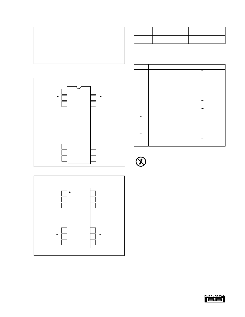
PACKAGE INFORMATION
(1)
PACKAGE DRAWING
NUMBER
MODEL
PACKAGE
ISO150AP
ISO150AU
NOTE: (1) For detailed drawing and dimension table, please see end of
data sheet, or Appendix D of Burr-Brown IC Data Book.
24-Pin Single-Wide DIP
28-Lead SOIC
243-1
217-2
PIN CONFIGURATION
TOP VIEW
DIP
24
23
22
15
14
13
1
2
3
10
11
12
D
1A
R/T
1A
V
SA
G
B
R/T
1B
D
1B
D
2A
R/T
2A
G
A
V
SB
R/T
2B
D
2B
TOP VIEW
SOIC
PIN DESCRIPTIONS
NAME
FUNCTION
D
1A
Data in or data out for transceiver 1A. R/T
1A
held
low makes D
1A
an input pin.
Receive/Transmit switch controlling transceiver 1A.
R/T
1A
V
SA
+5V supply pin for side A which powers transceivers
1A and 2A.
G
B
R/T
1B
D
1B
Ground pin for transceivers 1B and 2B.
Receive/Transmit switch controlling transceiver 1B.
Data in or data out for transceiver 1B. R/T
1B
held
low makes D
1B
an input pin.
Data in or data out for transceiver 2B. R/T
2B
held
low makes D
2B
an input pin.
Receive/Transmit switch controlling D
2B
.
+5V supply pin for side B which powers transceivers
1B and 2B.
D
2B
R/T
2B
V
SB
G
A
R/T
2A
D
2A
Ground pin for transceivers 1A and 2A.
Receive/Transmit switch controlling transceiver 2A.
Data in or data out for transceiver 2A. R/T
2A
held
low makes D
2A
in input pin.
ELECTROSTATIC
DISCHARGE SENSITIVITY
This integrated circuit can be damaged by ESD. Burr-Brown
recommends that all integrated circuits be handled with ap-
propriate precautions. Failure to observe proper handling and
installation procedures can cause damage.
ESD damage can range from subtle performance degradation
to complete device failure. Precision integrated circuits may
be more susceptible to damage because very small parametric
changes could cause the device not to meet its published
specifications.
28
27
26
17
16
15
1
2
3
12
13
14
D
1A
R/T
1A
V
SA
G
B
R/T
1B
D
1B
D
2A
R/T
2A
G
A
V
SB
R/T
2B
D
2B
相關(guān)PDF資料 |
PDF描述 |
|---|---|
| ISO150AP | Dual, Isolated, Bi-Directional DIGITAL COUPLER |
| ISO150AU | Dual, Isolated, Bi-Directional DIGITAL COUPLER |
| ISO164 | Precision, Isolated PROGRAMMABLE GAIN AMPLIFIER |
| ISO165 | Precision Instrumentation Amplifier |
| ISO166P | Precision, Isolated OPERATIONAL AMPLIFIER |
相關(guān)代理商/技術(shù)參數(shù) |
參數(shù)描述 |
|---|---|
| ISO150AP | 制造商:BB 制造商全稱:BB 功能描述:Dual, Isolated, Bi-Directional DIGITAL COUPLER |
| ISO150AU | 功能描述:隔離器接口集成電路 Dual Isol Bi-Dir Digital Coupler RoHS:否 制造商:Texas Instruments 通道數(shù)量:2 傳播延遲時(shí)間: 電源電壓-最大:5.5 V 電源電壓-最小:3 V 電源電流:3.6 mA 功率耗散: 最大工作溫度:+ 125 C 安裝風(fēng)格: 封裝 / 箱體:SOIC-8 封裝:Tube |
| ISO150AU | 制造商:Texas Instruments 功能描述:DUAL ISOLATED BIDIRECTIONAL DIGITAL COUP |
| ISO150AU/1K | 功能描述:隔離器接口集成電路 Dual Isol Bi-Dir Digital Coupler RoHS:否 制造商:Texas Instruments 通道數(shù)量:2 傳播延遲時(shí)間: 電源電壓-最大:5.5 V 電源電壓-最小:3 V 電源電流:3.6 mA 功率耗散: 最大工作溫度:+ 125 C 安裝風(fēng)格: 封裝 / 箱體:SOIC-8 封裝:Tube |
| ISO150AU/1KG4 | 功能描述:隔離器接口集成電路 Dual Isol Bi-Dir Digital Coupler RoHS:否 制造商:Texas Instruments 通道數(shù)量:2 傳播延遲時(shí)間: 電源電壓-最大:5.5 V 電源電壓-最小:3 V 電源電流:3.6 mA 功率耗散: 最大工作溫度:+ 125 C 安裝風(fēng)格: 封裝 / 箱體:SOIC-8 封裝:Tube |
發(fā)布緊急采購,3分鐘左右您將得到回復(fù)。