- 您現在的位置:買賣IC網 > PDF目錄360997 > ISO164 Precision, Isolated PROGRAMMABLE GAIN AMPLIFIER PDF資料下載
參數資料
| 型號: | ISO164 |
| 英文描述: | Precision, Isolated PROGRAMMABLE GAIN AMPLIFIER |
| 中文描述: | 精密,隔離可編程增益放大器 |
| 文件頁數: | 6/8頁 |
| 文件大小: | 194K |
| 代理商: | ISO164 |
6
ISO164/ISO174
Input-overload can produce an output voltage that appears
normal. For example, an input voltage of +20V on one input
and +40V on the other input will obviously exceed the linear
common-mode range of both input amplifiers. Since both
input amplifiers are saturated to nearly the same output
voltage limit, the difference voltage measured by the output
amplifier will be near zero. The output of the programmable-
gain amplifier will be near 0V even though both inputs are
overloaded.
INPUT PROTECTION
The inputs of the programmable-gain amplifiers are indi-
vidually protected for voltages up to
±
40V. For example, a
condition of –40V on one input and +40V on the other input
will not cause damage. Internal circuitry on each input
provides low series impedance under normal signal condi-
tions. To provide equivalent protection, series input resistors
would contribute excessive noise. If the input is overloaded,
the protection circuitry limits the input current to a safe
value (approximately 1.5mA). The inputs are protected even
if no power supply is present.
SYNCHRONIZED OPERATION
ISO164 and ISO174 can be synchronized to an external
signal source. This capability is useful in eliminating trouble-
some beat frequencies in multichannel systems and in reject-
ing AC signals and their harmonics. To use this feature, an
external signal must be applied to the Ext Osc pin. ISO164
can be synchronized over the 100kHz to 200kHz range and
ISO174 can be synchronized over the 400kHz to 700kHz
range.
BASIC OPERATION
ISO164 and ISO174 are comprised of a precision program-
mable gain amplifier followed by an isolation amplifier. The
input and output isolation sections are galvanically isolated
by matched and EMI shielded capacitors.
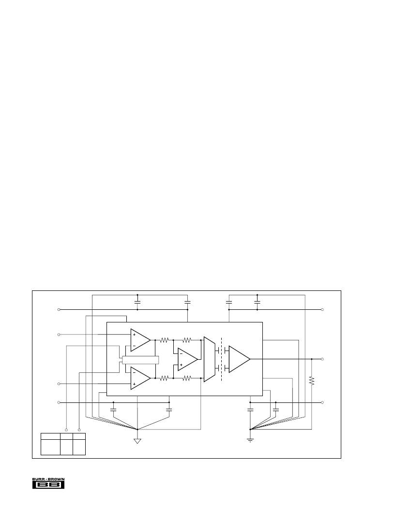
SIGNAL AND POWER CONNECTIONS
Figure 1 shows power and signal connections. Each power
supply pin should be bypassed with a 1
μ
F tantalum capaci-
tor located as close to the amplifier as possible. All ground
connections should be run independently to a common
point. Signal Common on both input and output sections
provide a high-impedance point for sensing signal ground in
noisy applications. Com 1 and Com 2 must have a path to
ground for bias current return and should be maintained
within
±
1V of GND 1 and GND 2 respectively.
INPUT COMMON-MODE RANGE
The linear common-mode range of the input circuitry of the
ISO164/174 is approximately
±
12.7V (or 2.3V from the
power supplies). As the output voltage increases, however,
the linear input range will be limited by the output voltage
swing of the internal amplifiers. Thus, the linear common-
mode range is related to the output voltage of the complete
input amplifier—see performance curves “Input Common-
Mode Range vs Output Voltage.”
A combination of common-mode and differential input
voltage can cause the output voltage of the internal amplifi-
ers to saturate. For applications where input common-mode
range must be maximized, limit the output voltage swing by
selecting a lower gain of the programmable-gain input.
FIGURE 1. Basic Connections.
V
IN–
Ext OSC
V
S1+
V
S2+
V
S1–
2
V
S2–
13
V
S2–
V
OUT
V
S2+
V
S1–
V
S1+
V
IN–
V
IN+
R
LOAD
20
Com 1/Shield 1
5
21
0.1μF
1μF
1
15
Shield 2
V
OUT
Com 2
14
11
10
A1
A0
V
IN+
3
24
23
4
GND 1
1μF
0.1μF
1μF
0.1μF
1μF
0.1μF
1
10
100
0
0
1
0
1
0
GAIN
A1
A0
22 DGND
GND 2 12
相關PDF資料 |
PDF描述 |
|---|---|
| ISO165 | Precision Instrumentation Amplifier |
| ISO166P | Precision, Isolated OPERATIONAL AMPLIFIER |
| ISO166 | |
| ISO175P | Single Supply, Rail-to-Rail, Low Cost Instrumentation Amplifier |
| ISO175 | Single Supply, Rail-to-Rail, Low Cost Instrumentation Amplifier |
相關代理商/技術參數 |
參數描述 |
|---|---|
| ISO164/ISO174 | 制造商:未知廠家 制造商全稱:未知廠家 功能描述:ISO164. ISO174 - DISCONTINUED PRODUCT. No longer recommended for new design. |
| ISO165 | 制造商:BB 制造商全稱:BB 功能描述:INSTRUMENTATION AMPLIFIER |
| ISO165/ISO175 | 制造商:未知廠家 制造商全稱:未知廠家 功能描述:ISO165. ISO175 - DISCONTINUED PRODUCT. No longer recommended for new design. |
| ISO166 | 制造商:未知廠家 制造商全稱:未知廠家 功能描述: |
| ISO166/ISO176 | 制造商:未知廠家 制造商全稱:未知廠家 功能描述:ISO166. ISO176 - DISCONTINUED PRODUCT. No longer recommended for new design. |
發布緊急采購,3分鐘左右您將得到回復。