- 您現在的位置:買賣IC網 > PDF目錄384535 > ISPGDX160VA-5B272 (LATTICE SEMICONDUCTOR CORP) In-System Programmable 3.3V Generic Digital CrosspointTM PDF資料下載
參數資料
| 型號: | ISPGDX160VA-5B272 |
| 廠商: | LATTICE SEMICONDUCTOR CORP |
| 元件分類: | PLD |
| 英文描述: | In-System Programmable 3.3V Generic Digital CrosspointTM |
| 中文描述: | EE PLD, 5 ns, PBGA272 |
| 封裝: | BGA-272 |
| 文件頁數: | 1/37頁 |
| 文件大小: | 464K |
| 代理商: | ISPGDX160VA-5B272 |
當前第1頁第2頁第3頁第4頁第5頁第6頁第7頁第8頁第9頁第10頁第11頁第12頁第13頁第14頁第15頁第16頁第17頁第18頁第19頁第20頁第21頁第22頁第23頁第24頁第25頁第26頁第27頁第28頁第29頁第30頁第31頁第32頁第33頁第34頁第35頁第36頁第37頁
1
ispGDX
TM
160V/VA
In-System Programmable
3.3V Generic Digital Crosspoint
TM
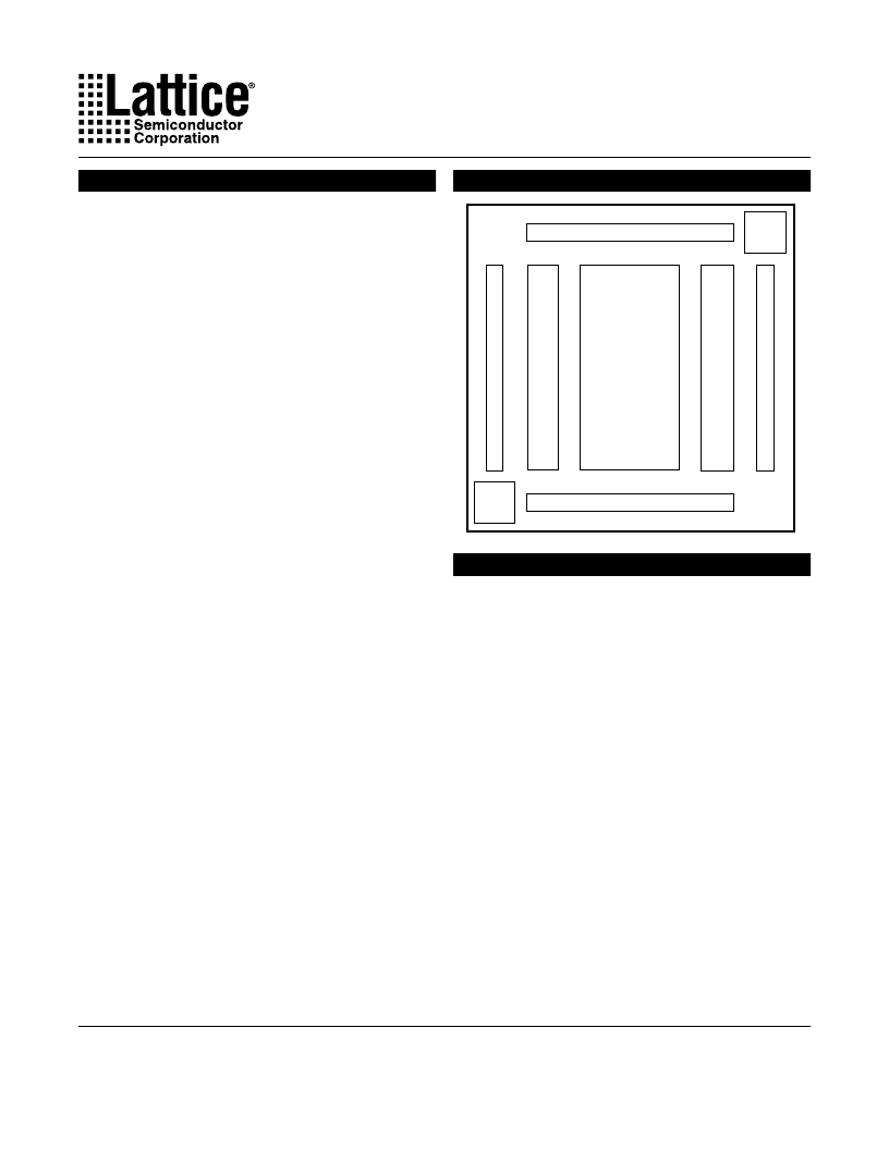
Functional Block Diagram
Features
IN-SYSTEM PROGRAMMABLE GENERIC DIGITAL
CROSSPOINT FAMILY
— Advanced Architecture Addresses Programmable
PCB Interconnect, Bus Interface Integration and
Jumper/Switch Replacement
— “Any Input to Any Output” Routing
— Fixed HIGH or LOW Output Option for Jumper/DIP
Switch Emulation
— Space-Saving PQFP and BGA Packaging
— Dedicated IEEE 1149.1-Compliant Boundary Scan
Test
HIGH PERFORMANCE E
2
CMOS
TECHNOLOGY
— 3.3V Core Power Supply
— 3.5ns Input-to-Output/3.5ns Clock-to-Output Delay*
— 250MHz Maximum Clock Frequency*
— TTL/3.3V/2.5V Compatible Input Thresholds and
Output Levels (Individually Programmable)*
— Low-Power: 16.5mA Quiescent Icc*
— 24mA I
OL
Drive with Programmable Slew Rate
Control Option
— PCI Compatible Drive Capability*
— Schmitt Trigger Inputs for Noise Immunity
— Electrically Erasable and Reprogrammable
— Non-Volatile E
2
CMOS Technology
ispGDXV OFFERS THE FOLLOWING ADVANTAGES
— 3.3V In-System Programmable Using Boundary Scan
Test Access Port (TAP)
— Change Interconnects in Seconds
FLEXIBLE ARCHITECTURE
— Combinatorial/Latched/Registered Inputs or Outputs
— Individual I/O Tri-state Control with Polarity Control
— Dedicated Clock/Clock Enable Input Pins (four) or
Programmable Clocks/Clock Enables from I/O Pins
(40)
— Single Level 4:1 Dynamic Path Selection (Tpd = 3.5ns)
— Programmable Wide-MUX Cascade Feature
Supports up to 16:1 MUX
— Programmable Pull-ups, Bus Hold Latch and Open
Drain on I/O Pins
— Outputs Tri-state During Power-up (“Live Insertion”
Friendly)
DESIGN SUPPORT THROUGH LATTICE’S ispGDX
DEVELOPMENT SOFTWARE
— MS Windows or NT / PC-Based or Sun O/S
— Easy Text-Based Design Entry
— Automatic Signal Routing
— Program up to 100 ISP Devices Concurrently
— Simulator Netlist Generation for Easy Board-Level
Simulation
* “VA” Version Only
Copyright 2000 Lattice Semiconductor Corporation. All brand or product names are trademarks or registered trademarks of their respective holders. The specifications and information herein
are subject to change without notice.
Global Routing
Pool
(GRP)
I/O
Cells
I/O Pins B
Boundary
Scan
Control
I/O
Cells
ISP
Control
I
I
I/O Pins D
Description
The ispGDXV/VA architecture provides a family of fast,
flexible programmable devices to address a variety of
system-level digital signal routing and interface require-
ments including:
Multi-Port Multiprocessor Interfaces
Wide Data and Address Bus Multiplexing
(e.g. 16:1 High-Speed Bus MUX)
Programmable Control Signal Routing
(e.g. Interrupts, DMAREQs, etc.)
Board-Level PCB Signal Routing for Prototyping or
Programmable Bus Interfaces
The devices feature fast operation, with input-to-output
signal delays (Tpd) of 3.5ns and clock-to-output delays of
3.5ns.
The architecture of the devices consists of a series of
programmable I/O cells interconnected by a Global Rout-
ing Pool (GRP). All I/O pin inputs enter the GRP directly
or are registered or latched so they can be routed to the
required I/O outputs. I/O pin inputs are defined as four
sets (A,B,C,D) which have access to the four MUX inputs
gdx160va_04
LATTICE SEMICONDUCTOR CORP., 5555 Northeast Moore Ct., Hillsboro, Oregon 97124, U.S.A.
Tel. (503) 268-8000; 1-800-LATTICE; FAX (503) 268-8556; http://www.latticesemi.com
July 2000
相關PDF資料 |
PDF描述 |
|---|---|
| ISPGDX160VA-5B272I | In-System Programmable 3.3V Generic Digital CrosspointTM |
| ISPGDX160VA-5Q208 | In-System Programmable 3.3V Generic Digital CrosspointTM |
| ISPGDX160VA-5Q208I | In-System Programmable 3.3V Generic Digital CrosspointTM |
| ISPGDX160V-5B208 | In-System Programmable 3.3V Generic Digital CrosspointTM |
| ISPGDX160V-5Q208 | In-System Programmable 3.3V Generic Digital CrosspointTM |
相關代理商/技術參數 |
參數描述 |
|---|---|
| ISPGDX160VA-5B272-7I | 制造商:Lattice Semiconductor Corporation 功能描述: |
| ISPGDX160VA-5B272I | 功能描述:模擬和數字交叉點 IC PROGRAMMABLE GEN DIG CROSSPOINT RoHS:否 制造商:Micrel 配置:2 x 2 封裝 / 箱體:MLF-16 數據速率:10.7 Gbps 輸入電平:CML, LVDS, LVPECL 輸出電平:CML 電源電壓-最大:3.6 V 電源電壓-最小:2.375 V 最大工作溫度:+ 85 C 最小工作溫度:- 40 C 產品:Digital Crosspoint 封裝:Tube |
| ISPGDX160VA-5BN208 | 功能描述:模擬和數字交叉點 IC PROGRAMMABLE GEN DIG CROSSPOINT RoHS:否 制造商:Micrel 配置:2 x 2 封裝 / 箱體:MLF-16 數據速率:10.7 Gbps 輸入電平:CML, LVDS, LVPECL 輸出電平:CML 電源電壓-最大:3.6 V 電源電壓-最小:2.375 V 最大工作溫度:+ 85 C 最小工作溫度:- 40 C 產品:Digital Crosspoint 封裝:Tube |
| ISPGDX160VA-5BN208I | 功能描述:模擬和數字交叉點 IC PROGRAMMABLE GEN DIG CROSSPOINT RoHS:否 制造商:Micrel 配置:2 x 2 封裝 / 箱體:MLF-16 數據速率:10.7 Gbps 輸入電平:CML, LVDS, LVPECL 輸出電平:CML 電源電壓-最大:3.6 V 電源電壓-最小:2.375 V 最大工作溫度:+ 85 C 最小工作溫度:- 40 C 產品:Digital Crosspoint 封裝:Tube |
| ISPGDX160VA-5Q208 | 功能描述:模擬和數字交叉點 IC 3.3V 160 I/O RoHS:否 制造商:Micrel 配置:2 x 2 封裝 / 箱體:MLF-16 數據速率:10.7 Gbps 輸入電平:CML, LVDS, LVPECL 輸出電平:CML 電源電壓-最大:3.6 V 電源電壓-最小:2.375 V 最大工作溫度:+ 85 C 最小工作溫度:- 40 C 產品:Digital Crosspoint 封裝:Tube |
發布緊急采購,3分鐘左右您將得到回復。