- 您現(xiàn)在的位置:買賣IC網(wǎng) > PDF目錄1930 > ISPLSI 5384VE-165LB272 (Lattice Semiconductor Corporation)IC PLD ISP 192I/O 6NS 272BGA PDF資料下載
參數(shù)資料
| 型號(hào): | ISPLSI 5384VE-165LB272 |
| 廠商: | Lattice Semiconductor Corporation |
| 文件頁數(shù): | 1/22頁 |
| 文件大小: | 0K |
| 描述: | IC PLD ISP 192I/O 6NS 272BGA |
| 標(biāo)準(zhǔn)包裝: | 40 |
| 系列: | ispLSI® 5000VE |
| 可編程類型: | 系統(tǒng)內(nèi)可編程 |
| 最大延遲時(shí)間 tpd(1): | 6.0ns |
| 電壓電源 - 內(nèi)部: | 3 V ~ 3.6 V |
| 邏輯元件/邏輯塊數(shù)目: | 12 |
| 宏單元數(shù): | 384 |
| 門數(shù): | 18000 |
| 輸入/輸出數(shù): | 192 |
| 工作溫度: | 0°C ~ 70°C |
| 安裝類型: | 表面貼裝 |
| 封裝/外殼: | 272-BBGA |
| 供應(yīng)商設(shè)備封裝: | 272-BGA(27x27) |
| 包裝: | 托盤 |
| 其它名稱: | ISPLSI5384VE-165LB272 |
ispLSI 5384VE
In-System Programmable
3.3V SuperWIDE High Density PLD
1
5384ve_05
Copyright 2002 Lattice Semiconductor Corp. All brand or product names are trademarks or registered trademarks of their respective holders. The specifications and information herein are subject
to change without notice.
LATTICE SEMICONDUCTOR CORP., 5555 Northeast Moore Ct., Hillsboro, Oregon 97124, U.S.A.
January 2002
Tel. (503) 268-8000; 1-800-LATTICE; FAX (503) 268-8556; http://www.latticesemi.com
Features
Second Generation SuperWIDE HIGH DENSITY
IN-SYSTEM PROGRAMMABLE LOGIC DEVICE
— 3.3V Power Supply
— User Selectable 3.3V/2.5V I/O
— 18000 PLD Gates / 384 Macrocells
— Up to 192 I/O Pins
— 384 Registers
— High-Speed Global Interconnect
— SuperWIDE Generic Logic Block (32 Macrocells) for
Optimum Performance
— SuperWIDE Input Gating (68 Inputs) for Fast
Counters, State Machines, Address Decoders, etc.
— PCB Efficient Ball Grid Array (BGA) Package Options
— Interfaces with Standard 5V TTL Devices
HIGH PERFORMANCE E2CMOS TECHNOLOGY
—
fmax = 165 MHz Maximum Operating Frequency
—
tpd = 6.0 ns Propagation Delay
— TTL/3.3V/2.5V Compatible Input Thresholds and
Output Levels
— Electrically Erasable and Reprogrammable
— Non-Volatile
— Programmable Speed/Power Logic Path Optimization
IN-SYSTEM PROGRAMMABLE
— Increased Manufacturing Yields, Reduced Time-to-
Market, and Improved Product Quality
— Reprogram Soldered Devices for Faster Debugging
100% IEEE 1149.1 BOUNDARY SCAN TESTABLE AND
3.3V IN-SYSTEM PROGRAMMABLE
ARCHITECTURE FEATURES
— Enhanced Pin-Locking Architecture with Single-
Level Global Routing Pool and SuperWIDE GLBs
— Wrap Around Product Term Sharing Array Supports
up to 35 Product Terms Per Macrocell
— Macrocells Support Concurrent Combinatorial and
Registered Functions
— Macrocell Registers Feature Multiple Control
Options Including Set, Reset and Clock Enable
— Four Dedicated Clock Input Pins Plus Macrocell
Product Term Clocks
— Programmable I/O Supports Programmable Bus
Hold, Pull-up, Open Drain and Slew Rate Options
— Four Global Product Term Output Enables, Two
Global OE Pins and One Product Term OE per
Macrocell
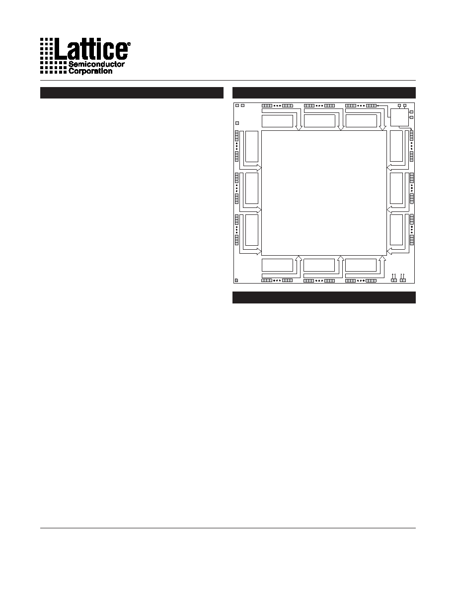
Global Routing Pool
(GRP)
Boundary
Scan
Interface
Input Bus
Generic
Logic Block
Input Bus
Generic
Logic Block
Input Bus
Generic
Logic Block
Generic
Logic Block
Generic
Logic Block
Generic
Logic Block
Input
Bus
Generic
Logic
Block
Input
Bus
Generic
Logic
Block
Input
Bus
Input
Bus
Input
Bus
Input
Bus
Generic
Logic
Block
Generic
Logic
Block
Generic
Logic
Block
Generic
Logic
Block
ispLSI 5000VE Description
The ispLSI 5000VE Family of In-System Programmable
High Density Logic Devices is based on Generic Logic
Blocks (GLBs) of 32 registered macrocells and a single
Global Routing Pool (GRP) structure interconnecting the
GLBs.
Outputs from the GLBs drive the Global Routing Pool
(GRP) between the GLBs. Switching resources are pro-
vided to allow signals in the Global Routing Pool to drive
any or all the GLBs in the device. This mechanism allows
fast, efficient connections across the entire device.
Each GLB contains 32 macrocells and a fully populated,
programmable AND-array with 160 logic product terms
and three extra control product terms. The GLB has 68
inputs from the Global Routing Pool which are available
in both true and complement form for every product term.
The 160 product terms are grouped in 32 sets of five and
sent into a Product Term Sharing Array (PTSA) which
allows sharing up to a maximum of 35 product terms for
a single function. Alternatively, the PTSA can be by-
passed for functions of five product terms or less. The
three extra product terms are used for shared controls:
reset, clock, clock enable and output enable.
Functional Block Diagram
相關(guān)PDF資料 |
PDF描述 |
|---|---|
| ISPLSI 5512VA-110LB388 | IC PLD ISP 288I/O 8.5NS 388BGA |
| ISPLSI 5512VE-155LB388 | IC PLD ISP 256I/O 6.5NS 388BGA |
| IXDP610PI | IC PWM CTRL BUS DIGITAL 18-PDIP |
| IXDP631PI | IC GENERATOR DGTL DEADTIME 8PDIP |
| JLC1562BFG | IC I/O EXPANDER I2C 8B 16SOEIAJ |
相關(guān)代理商/技術(shù)參數(shù) |
參數(shù)描述 |
|---|---|
| ISPLSI5384VE-165LB272 | 功能描述:CPLD - 復(fù)雜可編程邏輯器件 RoHS:否 制造商:Lattice 系列: 存儲(chǔ)類型:EEPROM 大電池?cái)?shù)量:128 最大工作頻率:333 MHz 延遲時(shí)間:2.7 ns 可編程輸入/輸出端數(shù)量:64 工作電源電壓:3.3 V 最大工作溫度:+ 90 C 最小工作溫度:0 C 封裝 / 箱體:TQFP-100 |
| ISPLSI5384VE-165LF256 | 功能描述:CPLD - 復(fù)雜可編程邏輯器件 RoHS:否 制造商:Lattice 系列: 存儲(chǔ)類型:EEPROM 大電池?cái)?shù)量:128 最大工作頻率:333 MHz 延遲時(shí)間:2.7 ns 可編程輸入/輸出端數(shù)量:64 工作電源電壓:3.3 V 最大工作溫度:+ 90 C 最小工作溫度:0 C 封裝 / 箱體:TQFP-100 |
| ISPLSI5384VE-80LB272I | 功能描述:CPLD - 復(fù)雜可編程邏輯器件 RoHS:否 制造商:Lattice 系列: 存儲(chǔ)類型:EEPROM 大電池?cái)?shù)量:128 最大工作頻率:333 MHz 延遲時(shí)間:2.7 ns 可編程輸入/輸出端數(shù)量:64 工作電源電壓:3.3 V 最大工作溫度:+ 90 C 最小工作溫度:0 C 封裝 / 箱體:TQFP-100 |
| ISPLSI5384VE-80LF256I | 功能描述:CPLD - 復(fù)雜可編程邏輯器件 RoHS:否 制造商:Lattice 系列: 存儲(chǔ)類型:EEPROM 大電池?cái)?shù)量:128 最大工作頻率:333 MHz 延遲時(shí)間:2.7 ns 可編程輸入/輸出端數(shù)量:64 工作電源電壓:3.3 V 最大工作溫度:+ 90 C 最小工作溫度:0 C 封裝 / 箱體:TQFP-100 |
| ISPLSI5512VA-100LB272 | 功能描述:CPLD - 復(fù)雜可編程邏輯器件 RoHS:否 制造商:Lattice 系列: 存儲(chǔ)類型:EEPROM 大電池?cái)?shù)量:128 最大工作頻率:333 MHz 延遲時(shí)間:2.7 ns 可編程輸入/輸出端數(shù)量:64 工作電源電壓:3.3 V 最大工作溫度:+ 90 C 最小工作溫度:0 C 封裝 / 箱體:TQFP-100 |
發(fā)布緊急采購,3分鐘左右您將得到回復(fù)。