- 您現在的位置:買賣IC網 > PDF目錄384540 > ISPLSI2064VE-100LT100 (LATTICE SEMICONDUCTOR CORP) CRYSTAL 16.0 MHZ 20PF SMD PDF資料下載
參數資料
| 型號: | ISPLSI2064VE-100LT100 |
| 廠商: | LATTICE SEMICONDUCTOR CORP |
| 元件分類: | PLD |
| 英文描述: | CRYSTAL 16.0 MHZ 20PF SMD |
| 中文描述: | EE PLD, 13 ns, PQFP100 |
| 封裝: | 14 X 14 MM, 0.50 MM PITCH, TQFP-100 |
| 文件頁數: | 1/15頁 |
| 文件大小: | 200K |
| 代理商: | ISPLSI2064VE-100LT100 |
ispLSI
3.3V In-System Programmable
High Density SuperFAST PLD
2064VE
2064ve_06
1
Features
SuperFAST HIGH DENSITY PROGRAMMABLE LOGIC
— 2000 PLD Gates
— 64 and 32 I/O Pin Versions, Four Dedicated Inputs
— 64 Registers
— High Speed Global Interconnect
— Wide Input Gating for Fast Counters, State
Machines, Address Decoders, etc.
— Small Logic Block Size for Random Logic
— 100% Functional, JEDEC and Pinout Compatible with
ispLSI 2064V Devices
3.3V LOW VOLTAGE 2064 ARCHITECTURE
— Interfaces with Standard 5V TTL Devices
HIGH-PERFORMANCE E
2
CMOS
TECHNOLOGY
—
f
max
= 280MHz* Maximum Operating Frequency
—
t
pd
= 3.5ns* Propagation Delay
— Electrically Erasable and Reprogrammable
— Non-Volatile
— 100% Tested at Time of Manufacture
— Unused Product Term Shutdown Saves Power
IN-SYSTEM PROGRAMMABLE
— 3.3V In-System Programmability (ISP) Using
Boundary Scan Test Access Port (TAP)
— Open-Drain Output Option for Flexible Bus Interface
Capability, Allowing Easy Implementation of Wired-OR
or Bus Arbitration Logic
— Increased Manufacturing Yields, Reduced Time-to-
Market and Improved Product Quality
— Reprogram Soldered Devices for Faster Prototyping
100% IEEE 1149.1 BOUNDARY SCAN TESTABLE
THE EASE OF USE AND FAST SYSTEM SPEED OF
PLDs WITH THE DENSITY AND FLEXIBILITY OF FPGAs
— Enhanced Pin Locking Capability
— Three Dedicated Clock Input Pins
— Synchronous and Asynchronous Clocks
— Programmable Output Slew Rate Control
— Flexible Pin Placement
— Optimized Global Routing Pool Provides Global
Interconnectivity
ispDesignEXPERT – LOGIC COMPILER AND COM-
PLETE ISP DEVICE DESIGN SYSTEMS FROM HDL
SYNTHESIS THROUGH IN-SYSTEM PROGRAMMING
— Superior Quality of Results
— Tightly Integrated with Leading CAE Vendor Tools
— Productivity Enhancing Timing Analyzer, Explore
Tools, Timing Simulator and ispANALYZER
— PC and UNIX Platforms
*Advanced Information
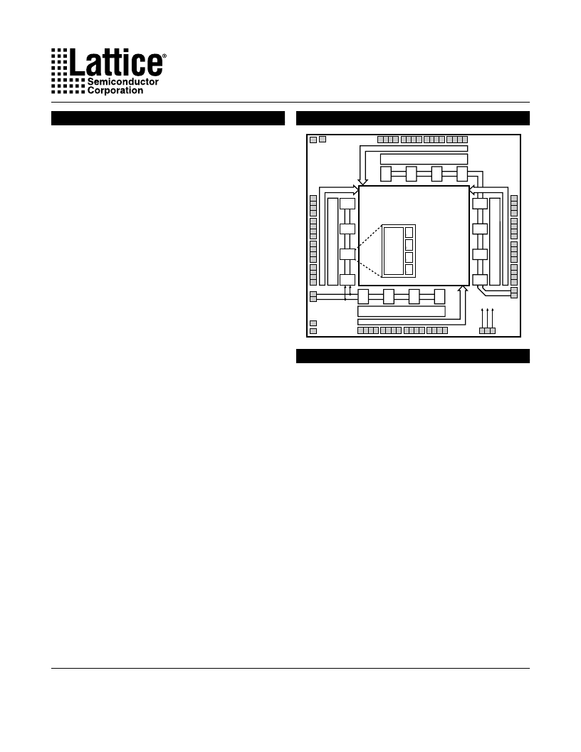
Functional Block Diagram
Global Routing Pool
(GRP)
A0
A1
A3
I
O
B3
B2
B1
B0
I
O
A2
GLB
Logic
Array
D Q
D Q
D Q
D Q
A4
A5
A6
A7
B7
B6
B5
B4
Input Bus
Output Routing Pool (ORP)
Input Bus
Output Routing Pool (ORP)
0139A/2064V
Description
The ispLSI 2064VE is a High Density Programmable
Logic Device available in 64 and 32 I/O-pin versions. The
device contains 64 Registers, four Dedicated Input pins,
three Dedicated Clock Input pins, two dedicated Global
OE input pins and a Global Routing Pool (GRP). The
GRP provides complete interconnectivity between all of
these elements. The ispLSI 2064VE features in-system
programmability through the Boundary Scan Test Ac-
cess Port (TAP) and is 100% IEEE 1149.1 Boundary
Scan Testable. The ispLSI 2064VE offers non-volatile
reprogrammability of the logic, as well as the intercon-
nect, to provide truly reconfigurable systems.
The basic unit of logic on the ispLSI 2064VE device is the
Generic Logic Block (GLB). The GLBs are labeled A0,
A1…B7 (see Figure 1). There are a total of 16 GLBs in the
ispLSI 2064VE device. Each GLB is made up of four
macrocells. Each GLB has 18 inputs, a programmable
AND/OR/Exclusive OR array, and four outputs which can
be configured to be either combinatorial or registered.
Inputs to the GLB come from the GRP and dedicated
inputs. All of the GLB outputs are brought back into the
GRP so that they can be connected to the inputs of any
GLB on the device.
Copyright 2000 Lattice Semiconductor Corp. All brand or product names are trademarks or registered trademarks of their respective holders. The specifications and information herein are subject
to change without notice.
LATTICE SEMICONDUCTOR CORP., 5555 Northeast Moore Ct., Hillsboro, Oregon 97124, U.S.A.
Tel. (503) 268-8000; 1-800-LATTICE; FAX (503) 268-8556; http://www.latticesemi.com
September 2000
相關PDF資料 |
PDF描述 |
|---|---|
| ISPLSI2064VE-100LT44 | CRYSTAL 16.0 MHZ 20PF SMD |
| ISPLSI2064VE-135LB100 | CRYSTAL 20.0 MHZ 20PF SMD |
| ISPLSI2064VE-135LT100 | 3.3V In-System Programmable High Density SuperFAST⑩ PLD |
| ISPLSI2064VE-135LT100I | 3.3V In-System Programmable High Density SuperFAST⑩ PLD |
| ISPLSI2064VE-135LT44 | 3.3V In-System Programmable High Density SuperFAST⑩ PLD |
相關代理商/技術參數 |
參數描述 |
|---|---|
| ISPLSI2064VE100LT44 | 制造商:LATTICE 功能描述:New |
| ISPLSI2064VE-100LT44 | 功能描述:CPLD - 復雜可編程邏輯器件 RoHS:否 制造商:Lattice 系列: 存儲類型:EEPROM 大電池數量:128 最大工作頻率:333 MHz 延遲時間:2.7 ns 可編程輸入/輸出端數量:64 工作電源電壓:3.3 V 最大工作溫度:+ 90 C 最小工作溫度:0 C 封裝 / 箱體:TQFP-100 |
| ISPLSI2064VE-100LTN100 | 功能描述:CPLD - 復雜可編程邏輯器件 RoHS:否 制造商:Lattice 系列: 存儲類型:EEPROM 大電池數量:128 最大工作頻率:333 MHz 延遲時間:2.7 ns 可編程輸入/輸出端數量:64 工作電源電壓:3.3 V 最大工作溫度:+ 90 C 最小工作溫度:0 C 封裝 / 箱體:TQFP-100 |
| ISPLSI2064VE-100LTN44 | 功能描述:CPLD - 復雜可編程邏輯器件 RoHS:否 制造商:Lattice 系列: 存儲類型:EEPROM 大電池數量:128 最大工作頻率:333 MHz 延遲時間:2.7 ns 可編程輸入/輸出端數量:64 工作電源電壓:3.3 V 最大工作溫度:+ 90 C 最小工作溫度:0 C 封裝 / 箱體:TQFP-100 |
| ISPLSI2064VE-135LB100 | 功能描述:CPLD - 復雜可編程邏輯器件 RoHS:否 制造商:Lattice 系列: 存儲類型:EEPROM 大電池數量:128 最大工作頻率:333 MHz 延遲時間:2.7 ns 可編程輸入/輸出端數量:64 工作電源電壓:3.3 V 最大工作溫度:+ 90 C 最小工作溫度:0 C 封裝 / 箱體:TQFP-100 |
發布緊急采購,3分鐘左右您將得到回復。