- 您現在的位置:買賣IC網 > PDF目錄377583 > L10C11PC15 (LOGIC DEVICES INC) Shift Register, Octal PDF資料下載
參數資料
| 型號: | L10C11PC15 |
| 廠商: | LOGIC DEVICES INC |
| 元件分類: | 數字信號處理外設 |
| 英文描述: | Shift Register, Octal |
| 中文描述: | 8-BIT, DSP-PIPELINE REGISTER, PDIP24 |
| 封裝: | 0.300 INCH, PLASTIC, DIP-24 |
| 文件頁數: | 1/6頁 |
| 文件大小: | 66K |
| 代理商: | L10C11PC15 |
DEVICES INCORPORATED
L10C11
4/8-bit Variable Length Shift Register
4/8-bit Variable Length Shift Register
Pipeline Registers
03/27/2000–LDS.11-L
1
K
Variable Length 4 or 8-bit Wide
Shift Register
K
Selectable Delay Length from 3 to
18 Stages
K
Low Power CMOS Technology
K
Replaces Fairchild TMC2011
K
Load, Shift, and Hold Instructions
K
Separate Data In and Data Out Pins
K
Package Styles Available:
24-pin Plastic DIP
28-pin Plastic LCC, J-Lead
FEATURES
DESCRIPTION
DEVICES INCORPORATED
The
L10C11
is a high-speed, low
power CMOS variable length shift
register. The L10C11
consists of two
4-bit wide, adjustable length shift
registers. These registers share control
signals and a common clock. Both
shift registers can be programmed
together to any length from 3 to 18
stages inclusive, or one register can be
fixed at 18 stages of delay while the
other is variable. The configuration
implemented is determined by the
Length Code (L
3-0
) and the MODE
control line as shown in Table 1.
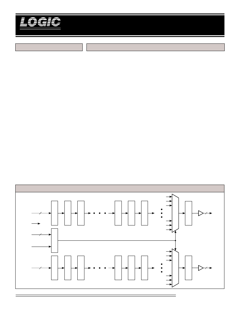
Each input is applied to a chain of
registers which are clocked on the
rising edge of the common CLK input.
These registers are numbered R1
through R17 and R1’ through R17’,
corresponding to the D
3-0
and D
7-4
data fields respectively. A multi-
plexer serves to route the contents of
any of registers R2 through R17 to the
output register, denoted R18. A
similar multiplexer operates on the
contents of R2’ through R17’ to load
R18’. Note that the minimum-length
path from data inputs to outputs is R1
to R2 to R18, consisting of three stages
of delay.
The MODE input determines whether
one or both of the internal shift
registers have variable length. When
MODE = 0, both D
3-0
and D
7-4
are
delayed by an amount which is
controlled by L
3-0
. When MODE = 1,
the D
7-4
field is delayed by 18 stages
independent of L
3-0
.
The Length Code (L
3-0
) controls the
number of stages of delay applied to
the D inputs as shown in Table 1.
When the Length Code is 0, the inputs
are delayed by 3 clock periods. When
the Length Code is 1, the delay is 4
clock periods, and so forth. The
Length Code and MODE inputs are
latched on the rising edge of CLK.
Both the Length Code and MODE
values may be changed at any time
without affecting the contents of
registers R1 through R17 or R1’
through R17’.
L10C11 B
LOCK
D
IAGRAM
R
R
R
R
R
R
L
D
3-0
4
R
R
R
R
R
R
D
7-4
4
L
3-0
MODE
4
CLK
R17
R16
R15
R4
R3
R2
M
R
4
Y
3-0
R
4
Y
7-4
R17’
R16’
R15’
R4’
R3’
R2’
M
相關PDF資料 |
PDF描述 |
|---|---|
| L10C11PC20 | Shift Register, Octal |
| L125 | SILICON GATE ENHANCEMENT MODE RF POWER LDMOS TRANSISTOR |
| L14C1 | HERMETIC SILICON PHOTOTRANSISTOR |
| L14C1 | HERMETIC SILICON PHOTOTRANSISTOR |
| L14C2 | HERMETIC SILICON PHOTOTRANSISTOR |
相關代理商/技術參數 |
參數描述 |
|---|---|
| L10C11PC20 | 制造商:LOGIC 制造商全稱:LOGIC 功能描述:Shift Register, Octal |
| L10C11PC25 | 制造商:未知廠家 制造商全稱:未知廠家 功能描述:Shift Register, Octal |
| L10C23CC20 | 制造商:未知廠家 制造商全稱:未知廠家 功能描述:Correlator |
| L10C23CC30 | 制造商:未知廠家 制造商全稱:未知廠家 功能描述:Correlator |
| L10C23CC50 | 制造商:未知廠家 制造商全稱:未知廠家 功能描述:Correlator |
發布緊急采購,3分鐘左右您將得到回復。