- 您現在的位置:買賣IC網 > PDF目錄30716 > LA3883M FM, AUDIO DEMODULATOR, PQFP48 PDF資料下載
參數資料
| 型號: | LA3883M |
| 元件分類: | 接收器 |
| 英文描述: | FM, AUDIO DEMODULATOR, PQFP48 |
| 封裝: | 14 X 14 MM, QIP-48 |
| 文件頁數: | 7/7頁 |
| 文件大小: | 117K |
| 代理商: | LA3883M |
LA3883M
PS No.A0794-7/7
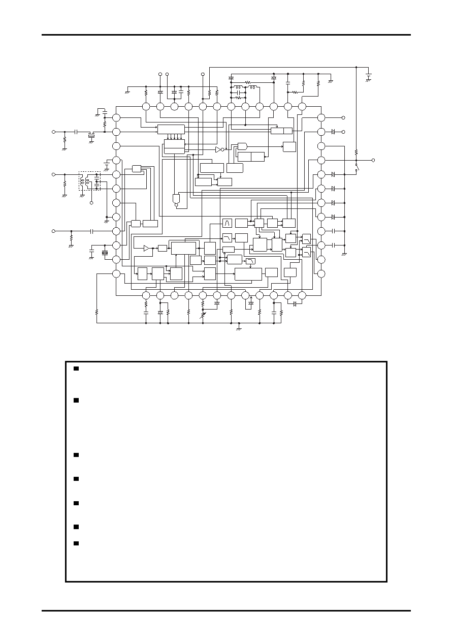
Block Diagram and Test Circuit
SANYO Semiconductor Co.,Ltd. assumes no responsibility for equipment failures that result from using
products at values that exceed, even momentarily, rated values (such as maximum ratings, operating condition
ranges, or other parameters) listed in products specifications of any and all SANYO Semiconductor Co.,Ltd.
products described or contained herein.
SANYO Semiconductor Co.,Ltd. strives to supply high-quality high-reliability products, however, any and all
semiconductor products fail or malfunction with some probability. It is possible that these probabilistic failures or
malfunction could give rise to accidents or events that could endanger human lives, trouble that could give rise
to smoke or fire, or accidents that could cause damage to other property. When designing equipment, adopt
safety measures so that these kinds of accidents or events cannot occur. Such measures include but are not
limited to protective circuits and error prevention circuits for safe design, redundant design, and structural
design.
Upon using the technical information or products described herein, neither warranty nor license shall be granted
with regard to intellectual property rights or any other rights of SANYO Semiconductor Co.,Ltd. or any third
party. SANYO Semiconductor Co.,Ltd. shall not be liable for any claim or suits with regard to a third party's
intellctual property rights which has resulted from the use of the technical information and products mentioned
above.
Information (including circuit diagrams and circuit parameters) herein is for example only; it is not guaranteed
for volume production.
Any and all information described or contained herein are subject to change without notice due to
product/technology improvement, etc. When designing equipment, refer to the "Delivery Specification" for the
SANYO Semiconductor Co.,Ltd. product that you intend to use.
In the event that any or all SANYO Semiconductor Co.,Ltd. products described or contained herein are
controlled under any of applicable local export control laws and regulations, such products may require the
export license from the authorities concerned in accordance with the above law.
No part of this publication may be reproduced or transmitted in any form or by any means, electronic or
mechanical, including photocopying and recording, or any information storage or retrieval system, or otherwise,
without the prior written consent of SANYO Semiconductor Co.,Ltd.
This catalog provides information as of May, 2007. Specifications and information herein are subject
to change without notice.
37
38
39
40
41
42
43
44
45
46
47
48
24
36
35
34
33
32
31
30
29
28
27
26
25
1
2
3
4
5
6
7
8
9
10
11
12
23
22
21
20
19
18
17
16
15
14
13
+
BUFFER
OSC
MIX
LPF
AMP
Q.DET
DC-C
DET
AFC
CIAMP
MUTE
DRIVE
HOLE
DET
MRC
CONT
MUTE
AMP
MUTE
AMP
DE-
ENPHA
SUBTRACTION
CIRCUIT
(MAIN)
SUBTRACTION
CIRCUIT
(SUB)
SUB
GATE
Control
BPF
3.5FH
TRAP
3.5FH
BPF
MAIN
GATE
Control
NOISE
DET
/AGC
HPF
PULSE
COUNT
2.7FH
BPF
1.3FH
BPF
DE-
ENPHA
Q-DET
PLL
CONT
DRIVER
HCC
SW
MATRIX
NOISE
AMP
CHARGE
DIS-CHARGE
330
Ω
50
Ω
330
Ω
0.047
μF
MIX
IN PUT
MIX-OUT
MUTE
FM-IF-IN
SFE10.7MS2-A
50
Ω
10pF
OSC-GND
0V
MAIN/SUB
DIVSRSITY
FM-IF-IN
IF-
OSC-VCC
22000pF
100k
Ω
10k
Ω
10k
Ω
100k
Ω
100k
Ω
1M
Ω
3.3k
Ω
1000pF
22k
Ω
2k
Ω
4.7
μF
1
μF
4.7
μF
4.7
μF
1000pF
+
51k
Ω
10k
Ω
100k
Ω
22k
Ω
15k
Ω
56k
Ω
10
μF
+
1
μF
2200pF
6.8k
Ω
22k
Ω
2k
Ω
0.022
μF
AFC-IN
22k
Ω
10
μF
+
10
μF
+
1
μF
+
1
μF
+
1
μF
2200pF
R
L
BIL-IND(Active-Low)
NC-IN
DET-OUT
SD-OUT
ST-IND
MRC-AC-IN
IF-VCC
MUTE
ATT
MUTE
DRIVE
STOP-REQ.
(SW3)
+
1
μF
+
0.47
μF
5V
SNC
IF
Limitter AMP
FM
S-METER
FM-SD
HCC
相關PDF資料 |
PDF描述 |
|---|---|
| LA4140 | 0.5 W, 1 CHANNEL, AUDIO AMPLIFIER, PSIP9 |
| LA4145 | 0.9 W, 2 CHANNEL, AUDIO AMPLIFIER, SIP9 |
| LA4147 | 0.9 W, 2 CHANNEL, AUDIO AMPLIFIER, SIP9 |
| LA4160 | 2.2 W, 1 CHANNEL, AUDIO AMPLIFIER, PDIP14 |
| LA4165M | SPECIALTY CONSUMER CIRCUIT, PDSO24 |
相關代理商/技術參數 |
參數描述 |
|---|---|
| LA-3893 | 制造商:Ideal Industries Inc 功能描述:FUSE, 2A / 600V |
| LA-3896 | 制造商:Ideal Industries Inc 功能描述:FUSE, 0.5A / 500V |
| LA-3897 | 制造商:Ideal Industries Inc 功能描述:FUSE, 10A / 600V |
| LA-3898 | 制造商:Ideal Industries Inc 功能描述:FUSE .1A / 250V |
| LA38B-125-EG-PF | 制造商:LIGITEK 制造商全稱:LIGITEK electronics co., ltd. 功能描述:LED ARRAY |
發布緊急采購,3分鐘左右您將得到回復。