- 您現在的位置:買賣IC網 > PDF目錄30718 > LA4628 30 W, 2 CHANNEL, AUDIO AMPLIFIER, PZFM14 PDF資料下載
參數資料
| 型號: | LA4628 |
| 元件分類: | 音頻/視頻放大 |
| 英文描述: | 30 W, 2 CHANNEL, AUDIO AMPLIFIER, PZFM14 |
| 封裝: | SIP-14 |
| 文件頁數: | 5/8頁 |
| 文件大小: | 125K |
| 代理商: | LA4628 |
LA4628
No.6632-5/8
3. Impulse noise improvements
While the LA4628 achieves a low level of impulse noise, if even further reductions in impulse noise at power on/off
(and when switching into or out of standby mode) a 0.47F capacitor may be inserted between pin 7 and the PRE
GND pin (pin 3). (Pin 7 is the output amplifier bias pin. Since the ability to withstand shorting the output pins to
VCC or ground is reduced for supply voltages over 16V if the pin 7 capacitance is large, we recommend a value of
0.47F or lower for this capacitor.)
4. Protection circuits
Due to the system structure of the protection circuit for shorts to VCC or ground, if there is a DC resistance between
the amplifier output pins and ground, the protection circuit may operate when power is first applied and the
amplifier may fail to turn on. The basic design approach we recommend is not to adopt any designs in which there is
a DC resistance between the amplifier outputs and ground.
The LA4628 includes a built-in thermal protection circuit to prevent the IC from being damaged or destroyed if
abnormally high temperatures occur. This thermal protection circuit gradually reduces the output if the IC junction
temperature (Tj) reaches the range 170 to 180
°C due to inadequate heat sinking or other problem. If the temperature
falls, the amplifier will restart automatically.
The LA4628 also includes other protection circuits. Use of these circuits also requires care during end product
design and testing.
5. Other notes
The LA4628 is a BTL power amplifier. When testing this device, the ground systems for the test equipment
connected to IC inputs, and that for the test equipment connected to IC outputs, must be isolated. Do not use a
common ground.
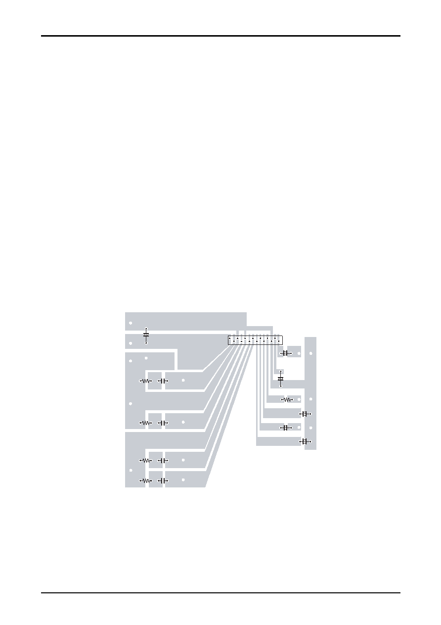
Printed Circuit Pattern
(copper foil side)
GND
VCC
GND
C5
R2
C6
-OUT1
C1
14
LA4628
1
+
IN1
IN2
C3
C2
R1
C4
C10
STB
+OUT1
-OUT2
+OUT2
R3
C7
R4
C8
R5
C9
相關PDF資料 |
PDF描述 |
|---|---|
| LA4629 | 4.5 W, 2 CHANNEL, AUDIO AMPLIFIER, SFM12 |
| LA4630N | 5 W, 3 CHANNEL, AUDIO AMPLIFIER, PSFM18 |
| LA4631 | 5 W, 2 CHANNEL, AUDIO AMPLIFIER, SFM13 |
| LA4631 | 5 W, 2 CHANNEL, AUDIO AMPLIFIER, SFM13 |
| LA4632 | 10 W, 2 CHANNEL, AUDIO AMPLIFIER, PSFM12 |
相關代理商/技術參數 |
參數描述 |
|---|---|
| LA4628_08 | 制造商:SANYO 制造商全稱:Sanyo Semicon Device 功能描述:For General Audio 20W 2-Channel BTL Power Amplifier |
| LA4628-E | 功能描述:音頻放大器 RoHS:否 制造商:STMicroelectronics 產品:General Purpose Audio Amplifiers 輸出類型:Digital 輸出功率: THD + 噪聲: 工作電源電壓:3.3 V 電源電流: 最大功率耗散: 最大工作溫度: 安裝風格:SMD/SMT 封裝 / 箱體:TQFP-64 封裝:Reel |
| LA4628L-E | 制造商:ON Semiconductor 功能描述:AUDIO AMPLIFIER BTL 2CH - Ammo Pack |
| LA4629 | 制造商:SANYO 制造商全稱:Sanyo Semicon Device 功能描述:Two-Channel Audio Frequency Power Amplifier |
| LA4630 | 制造商:未知廠家 制造商全稱:未知廠家 功能描述: |
發布緊急采購,3分鐘左右您將得到回復。