- 您現(xiàn)在的位置:買賣IC網(wǎng) > PDF目錄30721 > LA72702NV SPECIALTY CONSUMER CIRCUIT, PDSO24 PDF資料下載
參數(shù)資料
| 型號(hào): | LA72702NV |
| 元件分類: | 消費(fèi)家電 |
| 英文描述: | SPECIALTY CONSUMER CIRCUIT, PDSO24 |
| 封裝: | 0.275 INCH, SSOP-24 |
| 文件頁(yè)數(shù): | 10/10頁(yè) |
| 文件大小: | 155K |
| 代理商: | LA72702NV |
LA72702NV
No.A0979-9/10
Continued from preceding page.
Pin No.
Pin Name
Function
DC: voltage
AC: level
Equivalent Circuit
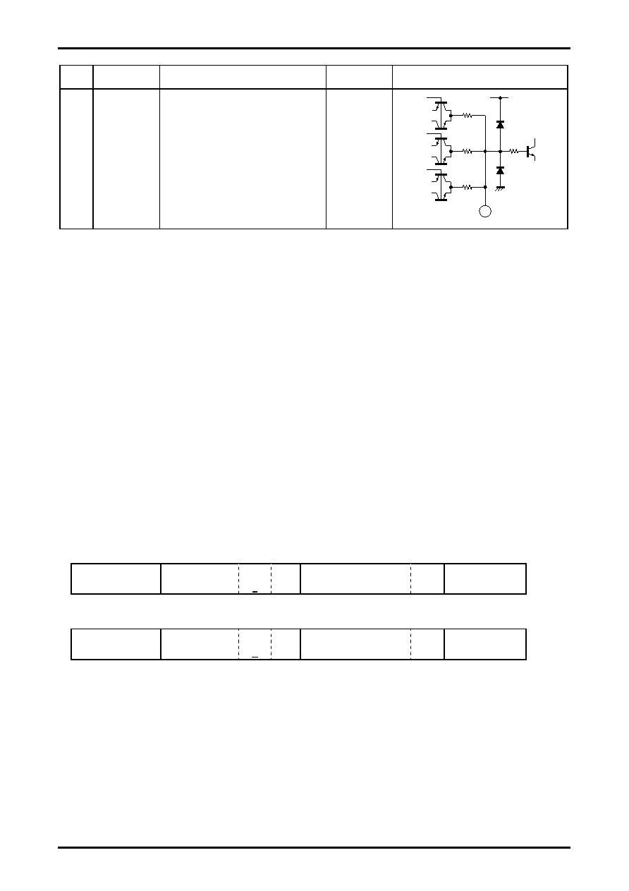
24
PCPTFILT
Pilot level detect for ST PLL filter
DC: 2.4V
I
2C BUS Serial Interface Specification
(1) Data transfer manual
This IC adopts control method (I
2C-BUS) with serial data, and controlled by two terminals which called SCL (serial
clock) and SDA (serial data).At first, set up
*1 the condition of starting data transfer, and after that, input 8 bit data to
SDA terminal with synchronized SCL terminal clock. The order of transferring is first, MSB (the Most Scale of Bit),
and save the order. The 9th bit takes ACK (Acknowledge) period, during SCL terminal takes ‘H’, this IC pull down the
SDA terminal. After transferred the necessary data, two terminals lead to set up and of
*2 data transfer stop condition,
thus the transfer comes to close.
*1 Defined by SCL rise down SDA during ‘H’ period.
*2 Defined by SCL rise up SDA during ‘H’ period.
(2) Transfer data format
After transfer start condition, transfers slave address (1000 000*) to SDA terminal, control data, then, stop condition
(See figure 1).
Slave address is made up of 7bits,
*38th bit shows the direction of transferring data, if it is ‘L’ takes write mode (As this
IC side, this is input operation mode), and in case of ‘H’ reading mode (As this IC side, this is output operation mode).
Data works with all of bit, transfer the stop condition before stop 8bit transfer, and to stop transfer, it will be canceled
the transfer dates.
*3 It is called R/W bit.
Fig.1 DATA STRUCTURE “WRITE” mode
START Condition
Slave Address
R/W
L
ACK
Control data
ACK
STOP condition
Fig.2 DATA STRUCTURE “READ” mode
START condition
Slave Address
R/W
H
ACK
Internal Data *
ACK
STOP condition
The output data synchronizes with the clock of SCL pin. Then, the ACK output is made after the output data.
bit8 is result of STERO DET (H : STEREO)
bit7 is result of SAP DET (H : SAP)
bit6 to bit1 are fixed to ‘L’
(3) Initialize
This IC is initialized for circuit protection. Initial condition is “0 (All bits) ”.
24
40k
Ω
40k
Ω
160k
Ω
1k
Ω
相關(guān)PDF資料 |
PDF描述 |
|---|---|
| LA72702NV | SPECIALTY CONSUMER CIRCUIT, PDSO24 |
| LA72702VA | SPECIALTY CONSUMER CIRCUIT, PDSO24 |
| LA7270 | 2 CHANNEL, VIDEO PREAMPLIFIER, PDIP22 |
| LA7270M | 2 CHANNEL, VIDEO PREAMPLIFIER, PDSO24 |
| LA72710V | SPECIALTY CONSUMER CIRCUIT, PDSO24 |
相關(guān)代理商/技術(shù)參數(shù) |
參數(shù)描述 |
|---|---|
| LA72702NV-MPB-E | 功能描述:編碼器、解碼器、復(fù)用器和解復(fù)用器 RoHS:否 制造商:Micrel 產(chǎn)品:Multiplexers 邏輯系列:CMOS 位數(shù): 線路數(shù)量(輸入/輸出):2 / 12 傳播延遲時(shí)間:350 ps, 400 ps 電源電壓-最大:2.625 V, 3.6 V 電源電壓-最小:2.375 V, 3 V 最大工作溫度:+ 85 C 安裝風(fēng)格:SMD/SMT 封裝 / 箱體:QFN-44 封裝:Tray |
| LA72702NV-TLM-E | 功能描述:編碼器、解碼器、復(fù)用器和解復(fù)用器 RoHS:否 制造商:Micrel 產(chǎn)品:Multiplexers 邏輯系列:CMOS 位數(shù): 線路數(shù)量(輸入/輸出):2 / 12 傳播延遲時(shí)間:350 ps, 400 ps 電源電壓-最大:2.625 V, 3.6 V 電源電壓-最小:2.375 V, 3 V 最大工作溫度:+ 85 C 安裝風(fēng)格:SMD/SMT 封裝 / 箱體:QFN-44 封裝:Tray |
| LA72702VA | 制造商:SANYO 制造商全稱:Sanyo Semicon Device 功能描述:Monolithic Linear IC For US TV BTSC Decoder |
| LA72703-E | 功能描述:音頻 DSP RoHS:否 制造商:Texas Instruments 工作電源電壓: 電源電流: 工作溫度范圍: 安裝風(fēng)格: 封裝 / 箱體: 封裝:Tube |
| LA72703V | 制造商:SANYO 制造商全稱:Sanyo Semicon Device 功能描述:Monolithic Linear IC For US TV BTSC Decoder |
發(fā)布緊急采購(gòu),3分鐘左右您將得到回復(fù)。