- 您現在的位置:買賣IC網 > PDF目錄30725 > LA76938Y SPECIALTY CONSUMER CIRCUIT, PDIP64 PDF資料下載
參數資料
| 型號: | LA76938Y |
| 元件分類: | 消費家電 |
| 英文描述: | SPECIALTY CONSUMER CIRCUIT, PDIP64 |
| 封裝: | 0.600 INCH, DIP-64 |
| 文件頁數: | 2/6頁 |
| 文件大小: | 115K |
| 代理商: | LA76938Y |
LA7693X series
No.A1102-2/6
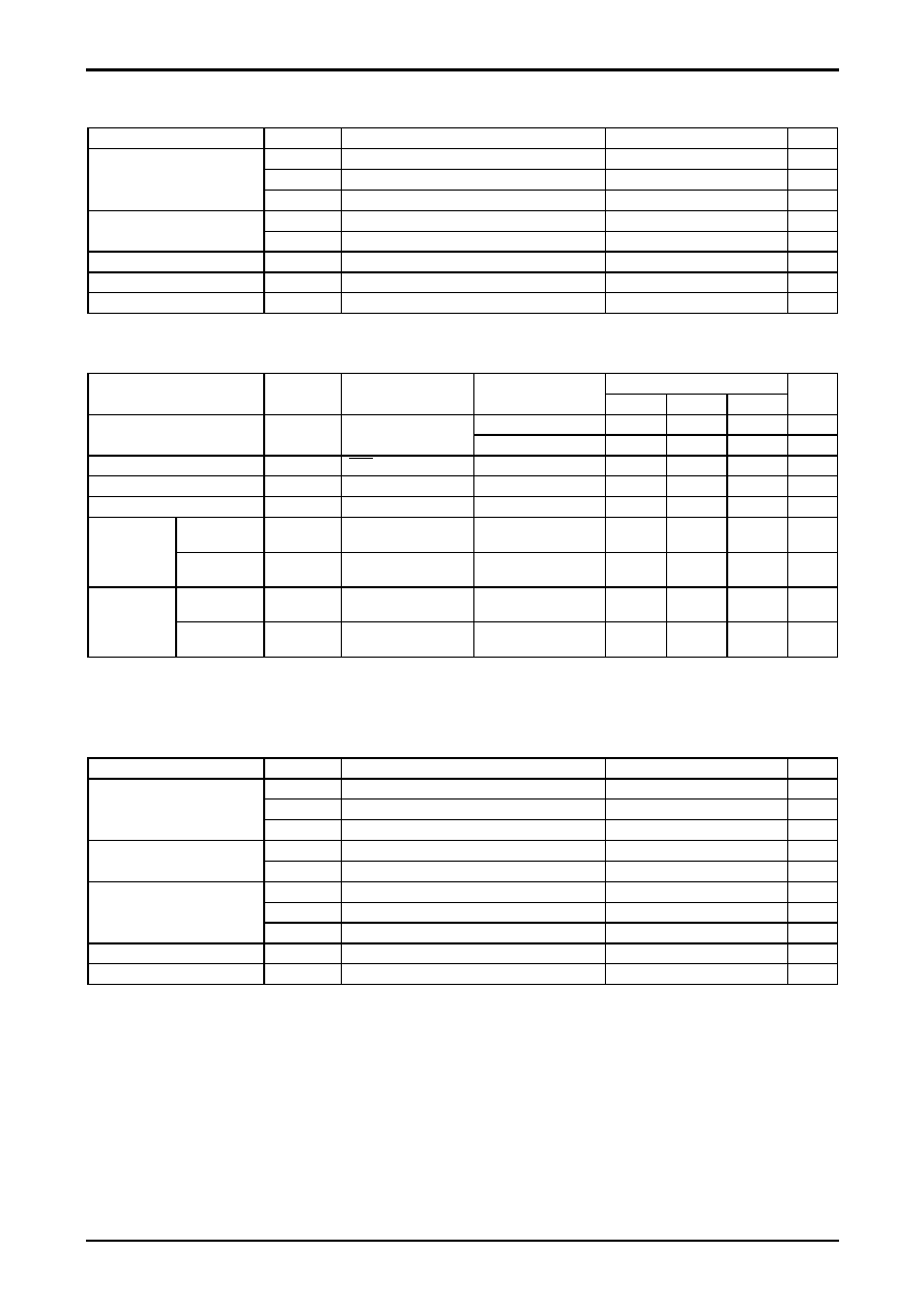
Specifications
Maximum Ratings (BIP Chip) at Ta = 25
°C
Parameter
Symbol
Conditions
Ratings
Unit
V8 max
7.0
V
V43 max
7.0
V
Maximum supply voltage
V55 max
7.0
V
I11 max
25
mA
Maximum supply current
I19 max
35
mA
Allowable power dissipation
Pd max
Ta
≤ 65°C *
1.6
W
Operating temperature
Topr
-10 to +65
°C
Storage temperature
Tstg
-55 to +150
°C
* Mounted on a substrate : 213mm
×140mm×1.6mm, glass epoxy board.
Absolute Maximum Ratings (Micro-computer Chip) at Ta
= 25°C, VSS = 0V
Ratings
Parameter
Symbol
Pins
Conditions
min
typ
max
Unit
Mask
-0.3
+6.0
V
Maximum supply voltege
VDD max
VDD
Flash
-0.3
+6.5
V
Input voltege
VI
RES
-0.3
VDD+0.3
V
Output voltege
VO
FILT
-0.3
VDD+0.3
V
Input/output voltege
VIO
Ports0, 1
-0.3
VDD+0.3
V
Peak output
current *2
IOPH
Ports04 to 07, 1
CMOS output
For each pin.
-4
mA
High level
output current
Total output
current
ΣIOAH
Ports04 to 07, 1
The total of all pins.
-15
mA
Peak output
current *2
IOPL
Ports0, 1
For cach pin
20
mA
Low lever
output current
Toral output
current
ΣIOAL
Ports0, 1
The total of all pins.
30
mA
*1
J : unted on a MASKROM = 24KB, K : MASKROM = 28KB, L : MASKROM = 32KB, M : MASKROM = 40KB, N : MASKROM = 48KB
FB : FLASHROM = 48KB (This production is produced and sold by SANYO under license of the Silicon Storage Technology Inc.)
*2
The average current for each pin must not be over 1mA.
Operating Conditions (Bip Chip) at Ta
= 25°C
Parameter
Symbol
Conditions
Ratings
Unit
V8
5.0
V
V43
5.0
V
Recommended supply voltege
V55
5.0
V
I11
19
mA
Recommended supply current
I19
31
mA
V8 op
4.7 to 5.3
V
V43 op
4.7 to 5.3
V
Operating supply voltege range
V55 op
4.7 to 5.3
V
Operating supply current range
I11 op
28 to 34
mA
I19 op
17 to 21
mA
相關PDF資料 |
PDF描述 |
|---|---|
| LA76936Y | SPECIALTY CONSUMER CIRCUIT, PDIP64 |
| LA76931J | SPECIALTY CONSUMER CIRCUIT, PDIP64 |
| LA76933J | SPECIALTY CONSUMER CIRCUIT, PDIP64 |
| LA7696 | ON-SCREEN DISPLAY IC, PDIP20 |
| LA7698 | SPECIALTY CONSUMER CIRCUIT, PDIP24 |
相關代理商/技術參數 |
參數描述 |
|---|---|
| LA76938Y7N59R1-E | 制造商:Sony Semiconductor Solutions Division 功能描述: |
| LA7696 | 制造商:SANYO 制造商全稱:Sanyo Semicon Device 功能描述:Color TV ON-Screen Display Interface |
| LA769670C59M7-E | 制造商:Sony Semiconductor Solutions Division 功能描述: |
| LA7698 | 制造商:SANYO 制造商全稱:Sanyo Semicon Device 功能描述:Color-Difference Signal Correction IC for Color TVs |
| LA-77 | 制造商:Chemence Ltd 功能描述:RS POLYOLEFIN PRIMER |
發布緊急采購,3分鐘左右您將得到回復。