- 您現在的位置:買賣IC網 > PDF目錄367527 > LC3564B-70 x8 SRAM PDF資料下載
參數資料
| 型號: | LC3564B-70 |
| 英文描述: | x8 SRAM |
| 中文描述: | x8的SRAM |
| 文件頁數: | 8/9頁 |
| 文件大小: | 145K |
| 代理商: | LC3564B-70 |
No. 5804-8/9
LC3564B, BS, BM, BT-70/10
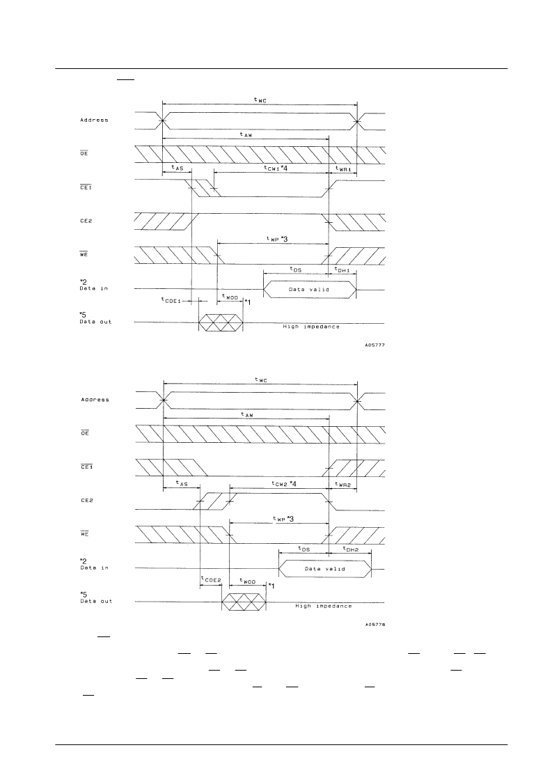
Write Cycle (2): CE1 Write *6
Write Cycle (3): CE2 Write *6
Notes: 1. Hold WE high during the read cycle.
2. Applications must not apply reverse phase signals to the D
OUT
pins when those pins are in the output state.
3. The time tWP is the period when CE1 and WE are low and CE2 is high, and is defined as the time from the fall of WE until either CE1 or WE rises,
or CE2 falls, whichever occurs first.
4. The times t
CW1
and t
CW2
are periods when CE1 and WE are low and CE2 is high. They are defined as the times from the fall of CE1 or the rise of
CE2 to the rise of CE1 and WE, or the fall of CE2, whichever occurs first.
5. The D
OUT
pins will be in the high-impedance state if either OE is high, CE1 is high, CE2 is low, or WE is low.
6. OE must be held either at V
IH
or V
IL
during the write cycle.
7. The D
OUT
pins have the same phase as the write cycle write data.
相關PDF資料 |
PDF描述 |
|---|---|
| LC3564BM-10 | |
| LC3564CT-70U | |
| LC3564P_SERIES | |
| LC3564PL-10 | |
| LC3564PL-12 | |
相關代理商/技術參數 |
參數描述 |
|---|---|
| LC3564BM | 制造商:SANYO 制造商全稱:Sanyo Semicon Device 功能描述:64K (8192-word ⅴ 8-bit) SRAM with OE, CE1, and CE2 Control Pins |
| LC3564BM-10 | 制造商:未知廠家 制造商全稱:未知廠家 功能描述: |
| LC3564BM-70 | 制造商:未知廠家 制造商全稱:未知廠家 功能描述:x8 SRAM |
| LC3564BS | 制造商:SANYO 制造商全稱:Sanyo Semicon Device 功能描述:64K (8192-word ⅴ 8-bit) SRAM with OE, CE1, and CE2 Control Pins |
| LC3564BS-10 | 制造商:未知廠家 制造商全稱:未知廠家 功能描述: |
發布緊急采購,3分鐘左右您將得到回復。