- 您現(xiàn)在的位置:買(mǎi)賣(mài)IC網(wǎng) > PDF目錄367535 > LC4102-T2A PDF資料下載
參數(shù)資料
| 型號(hào): | LC4102-T2A |
| 文件頁(yè)數(shù): | 3/8頁(yè) |
| 文件大小: | 68K |
| 代理商: | LC4102-T2A |
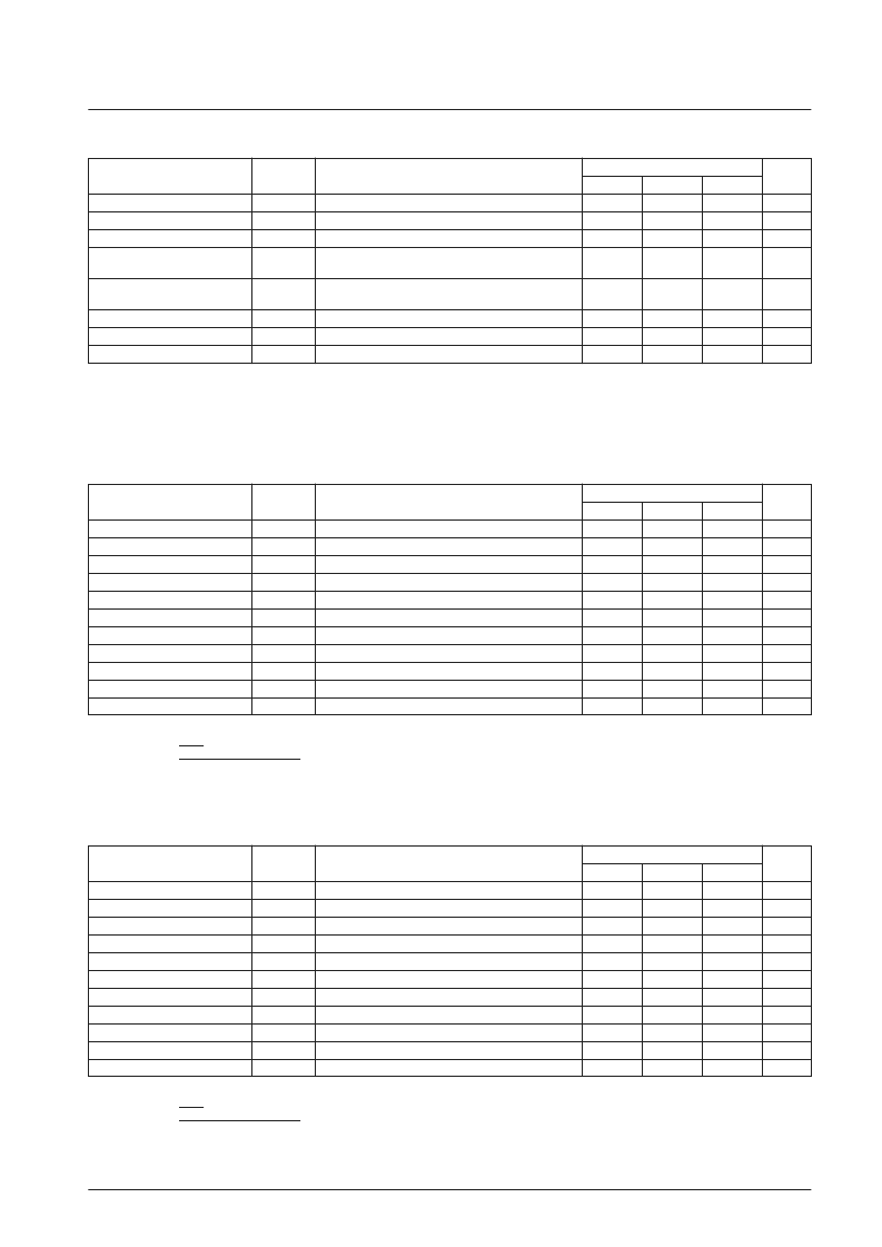
Allowable Operating Ranges
at Ta = –20 to +75°C, V
SS
= 0 V
Note: V0, V2, V3, and V5 must obey the following relationships: V
DDH
≥
V0
≥
V2
≥
V
DDH
– 7 V, and 7 V
≥
V3
≥
V5
≥
V
SS
.
At power on: First turn on the logic system power supply and then turn on the high-voltage system power supply; alternatively, turn both on at the
same time.
At power off: First turn off the high-voltage system power supply and then turn off the logic system power supply; alternatively, turn both off at the
same time.
Allowable Operating Ranges
at Ta = –20 to +75°C, V
SS
= 0 V, V
DD
= 5 V ± 10%
Note:
*
The clock rise time (tr) and fall time (tf) must obey inequalities
and
y
below.
1
– tw (cph) – tw (cpl)
fcp
2
: tr, tf <
y
: tr, tf
≤
50 ns
Allowable Operating Ranges
at Ta = –20 to +75°C, V
SS
= 0 V, V
DD
= 2.7 to 4.5 V
Note:
*
The clock rise time (tr) and fall time (tf) must obey inequalities
and
y
below.
1
– tw (cph) – tw (cpl)
fcp
2
: tr, tf <
y
: tr, tf
≤
50 ns
No. 6790-3/8
LC4104C-T2A
Parameter
Symbol
Conditions
Ratings
Unit
min
typ
max
Supply voltage
V
DD
V
DDH
V
SS
2.7
5.5
V
Supply voltage
14
36
V
Supply voltage
0
V
Input high-level voltage
V
IH
D0 to D7, LOAD, CP, R/L, M, TEST, DISP, BS,
EIO1, EIO2
0.8 V
DD
V
DD
V
Input low-level voltage
V
IL
D0 to D7, LOAD, CP, R/L, M, TEST, DISP, BS,
EIO1, EIO2
0
0.2 V
DD
V
Input voltage
V0, V2
V0, V2
V
DDH
– 7
V
DDH
V
Input voltage
V3
V3
0
V
SSH
+ 7
V
Input voltage
V5
V5
0
V
Parameter
Symbol
Conditions
Ratings
Unit
min
typ
max
CP clock frequency
fcp
CP
12
MHz
High-level load pulse width
tw (ldH)
LOAD
50
ns
High-level clock pulse width
tw (cpH)
CP
20
ns
Low-level clock pulse width
tw (cpL)
CP
20
ns
LOAD/CP setup time
tsu (ld)
LOAD, CP
100
ns
LOAD/CP hold time
tho (ld)
LOAD, CP
200
ns
DATA/CP setup time
tsu (cp)
CP, D0 to D7
10
ns
DATA/CP hold time
tho (cp)
CP, D0 to D7
10
ns
EIO input setup time
tsu (ei)
CP, EIO1, EIO2
24
ns
Clock rise time
tr
LOAD, CP
*
50
ns
Clock fall time
tf
LOAD, CP
*
50
ns
Parameter
Symbol
Conditions
Ratings
Unit
min
typ
max
CP clock frequency
fcp
CP
10
MHz
High-level load pulse width
tw (ldH)
LOAD
50
ns
High-level clock pulse width
tw (cpH)
CP
37
ns
Low-level clock pulse width
tw (cpL)
CP
37
ns
LOAD/CP setup time
tsu (ld)
LOAD, CP
100
ns
LOAD/CP hold time
tho (ld)
LOAD, CP
200
ns
DATA/CP setup time
tsu (cp)
CP, D0 to D7
35
ns
DATA/CP hold time
tho (cp)
CP, D0 to D7
35
ns
EIO input setup time
tsu (ei)
CP, EIO1, EIO2
30
ns
Clock rise time
tr
LOAD, CP
*
50
ns
Clock fall time
tf
LOAD, CP
*
50
ns
相關(guān)PDF資料 |
PDF描述 |
|---|---|
| LC4512B | Interface IC |
| LC4584B | Logic IC |
| LC4913 | Logic IC |
| LC4969 | Logic IC |
| LC506MCRO | Analog IC |
相關(guān)代理商/技術(shù)參數(shù) |
參數(shù)描述 |
|---|---|
| LC4103C | 制造商:SANYO 制造商全稱(chēng):Sanyo Semicon Device 功能描述:STN LCD Dot Matrix Common Driver |
| LC4103TAB-01 | 制造商:SANYO 制造商全稱(chēng):Sanyo Semicon Device 功能描述:STN LCD Dot Matrix Common Driver |
| LC4103TAB-02 | 制造商:SANYO 制造商全稱(chēng):Sanyo Semicon Device 功能描述:STN LCD Dot Matrix Common Driver |
| LC4104C | 制造商:SANYO 制造商全稱(chēng):Sanyo Semicon Device 功能描述:LCD Dot Matrix Segment Driver for STN Displays |
| LC4104C-T2A | 制造商:未知廠(chǎng)家 制造商全稱(chēng):未知廠(chǎng)家 功能描述: |
發(fā)布緊急采購(gòu),3分鐘左右您將得到回復(fù)。