- 您現在的位置:買賣IC網 > PDF目錄367534 > LC4256B-5F256AC PDF資料下載
參數資料
| 型號: | LC4256B-5F256AC |
| 文件頁數: | 2/57頁 |
| 文件大小: | 1078K |
| 代理商: | LC4256B-5F256AC |
第1頁當前第2頁第3頁第4頁第5頁第6頁第7頁第8頁第9頁第10頁第11頁第12頁第13頁第14頁第15頁第16頁第17頁第18頁第19頁第20頁第21頁第22頁第23頁第24頁第25頁第26頁第27頁第28頁第29頁第30頁第31頁第32頁第33頁第34頁第35頁第36頁第37頁第38頁第39頁第40頁第41頁第42頁第43頁第44頁第45頁第46頁第47頁第48頁第49頁第50頁第51頁第52頁第53頁第54頁第55頁第56頁第57頁
Lattice Semiconductor
ispMACH 4000V/B/C Family Data Sheet
2
ispMACH 4000 Introduction
The high performance ispMACH 4000 family from Lattice offers a SuperFAST CPLD solution. The family is a blend
of Lattice’s two most popular architectures: the ispLSI
2000 and ispMACH 4A. Retaining the best of both families,
the ispMACH 4000 architecture focuses on signi
fi
cant innovations to combine the highest performance with low
power in a
fl
exible CPLD family.
The ispMACH 4000 combines high speed and low power with the
fl
exibility needed for ease of design. With its
robust Global Routing Pool and Output Routing Pool, this family delivers excellent First-Time-Fit, timing predictabil-
ity, routing, pin-out retention and density migration.
The ispMACH 4000 family offers densities ranging from 32 to 512 macrocells. There are multiple density-I/O com-
binations in Thin Quad Flat Pack (TQFP) and Fine Pitch BGA (fpBGA) packages ranging from 44 to 256 pins/balls.
Table 1 shows the macrocell, package and I/O options, along with other key parameters.
The ispMACH 4000 family has enhanced system integration capabilities. It supports 3.3V (4000V), 2.5V (4000B)
and 1.8V (4000C) supply voltages and 3.3V, 2.5V and 1.8V interface voltages. The ispMACH 4000 also offers
enhanced I/O features such as slew rate control, PCI compatibility, bus-keeper latches, pull-up resistors, pull-down
resistors, open drain outputs and hot socketing. The ispMACH 4000 family members are 3.3V/2.5V/1.8V in-system
programmable through the IEEE Standard 1532 interface. IEEE Standard 1149.1 boundary scan testing capability
also allows product testing on automated test equipment.
Overview
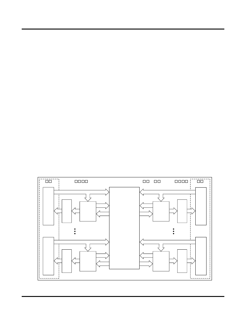
The ispMACH 4000 devices consist of multiple 36-input, 16-macrocell Generic Logic Blocks (GLBs) interconnected
by a Global Routing Pool (GRP). Output Routing Pools (ORPs) connect the GLBs to the I/O Blocks (IOBs), which
contain multiple I/O cells. This architecture is shown in Figure 1.
Figure 1. Functional Block Diagram
I/O
Block
ORP
ORP
16
16
G
G
V
C
G
T
T
T
T
36
Generic
Logic
Block
Generic
Logic
Block
I/O
Block
ORP
ORP
16
36
Generic
Logic
Block
Generic
Logic
Block
I/O
Block
I
I
I/O
Block
36
36
C
C
C
C
16
16
G
V
C
G
V
C
G
16
16
16
相關PDF資料 |
PDF描述 |
|---|---|
| LC4256B-5F256AI | |
| LC4256B-5T100C | |
| LC4256B-5T100I | |
| LC4256B-5T176C | |
| LC4256B-5T176I | |
相關代理商/技術參數 |
參數描述 |
|---|---|
| LC4256B-5F256AC1 | 制造商:LATTICE 制造商全稱:Lattice Semiconductor 功能描述:3.3V/2.5V/1.8V In-System Programmable SuperFAST High Density PLDs |
| LC4256B-5F256AI | 功能描述:CPLD - 復雜可編程邏輯器件 PROGRAMMABLE SUPER FAST HI DENSITY PLD RoHS:否 制造商:Lattice 系列: 存儲類型:EEPROM 大電池數量:128 最大工作頻率:333 MHz 延遲時間:2.7 ns 可編程輸入/輸出端數量:64 工作電源電壓:3.3 V 最大工作溫度:+ 90 C 最小工作溫度:0 C 封裝 / 箱體:TQFP-100 |
| LC4256B-5F256AI1 | 制造商:LATTICE 制造商全稱:Lattice Semiconductor 功能描述:3.3V/2.5V/1.8V In-System Programmable SuperFAST High Density PLDs |
| LC4256B-5F256BC | 功能描述:CPLD - 復雜可編程邏輯器件 PROGRAMMABLE SUPER FAST HI DENSITY PLD RoHS:否 制造商:Lattice 系列: 存儲類型:EEPROM 大電池數量:128 最大工作頻率:333 MHz 延遲時間:2.7 ns 可編程輸入/輸出端數量:64 工作電源電壓:3.3 V 最大工作溫度:+ 90 C 最小工作溫度:0 C 封裝 / 箱體:TQFP-100 |
| LC4256B-5F256BC1 | 制造商:LATTICE 制造商全稱:Lattice Semiconductor 功能描述:3.3V/2.5V/1.8V In-System Programmable SuperFAST High Density PLDs |
發布緊急采購,3分鐘左右您將得到回復。