- 您現(xiàn)在的位置:買賣IC網(wǎng) > PDF目錄367535 > LC4384V-75F256I PDF資料下載
參數(shù)資料
| 型號: | LC4384V-75F256I |
| 文件頁數(shù): | 6/57頁 |
| 文件大小: | 1078K |
| 代理商: | LC4384V-75F256I |
第1頁第2頁第3頁第4頁第5頁當(dāng)前第6頁第7頁第8頁第9頁第10頁第11頁第12頁第13頁第14頁第15頁第16頁第17頁第18頁第19頁第20頁第21頁第22頁第23頁第24頁第25頁第26頁第27頁第28頁第29頁第30頁第31頁第32頁第33頁第34頁第35頁第36頁第37頁第38頁第39頁第40頁第41頁第42頁第43頁第44頁第45頁第46頁第47頁第48頁第49頁第50頁第51頁第52頁第53頁第54頁第55頁第56頁第57頁
Lattice Semiconductor
ispMACH 4000V/B/C Family Data Sheet
6
Table 4. Product Term Expansion Capability
Every time the super cluster allocator is used, there is an incremental delay of t
tor is used, all destinations other than the one being steered to, are given the value of ground (i.e., if the super clus-
ter is steered to M (n+4), then M (n) is ground).
EXP
. When the super cluster alloca-
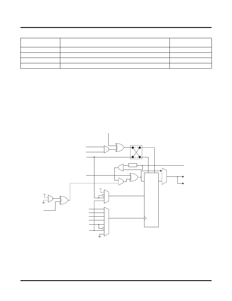
Macrocell
The 16 macrocells in the GLB are driven by the 16 outputs from the logic allocator. Each macrocell contains a pro-
grammable XOR gate, a programmable register/latch, along with routing for the logic and control functions. Figure
5 shows a graphical representation of the macrocell. The macrocells feed the ORP and GRP. A direct input from
the I/O cell allows designers to use the macrocell to construct high-speed input registers. A programmable delay in
this path allows designers to choose between the fastest possible set-up time and zero hold time.
Figure 5. Macrocell
Enhanced Clock Multiplexer
The clock input to the
fl
ip-
fl
op can select any of the four block clocks along with the shared PT clock, and true and
complement forms of the optional individual term clock. An 8:1 multiplexer structure is used to select the clock. The
eight sources for the clock multiplexer are as follows:
Block CLK0
Block CLK1
Expansion
Chains
Chain-0
Chain-1
Chain-2
Chain-3
Macrocells Associated with Expansion Chain
(with Wrap Around)
M0
→
M4
→
M8
M1
→
M5
→
M9
M2
→
M6
→
M10
M3
→
M7
→
M11
Max PT/
Macrocell
75
80
75
70
→
M12
M13
M14
M15
→
M0
M1
M2
M3
→
→
→
→
→
→
Single PT
Block CLK0
Block CLK1
Block CLK2
Block CLK3
PT Clock (optional)
Shared PT Clock
CE
D/T/L
Q
R
P
Shared PT Initialization
PT Initialization/CE (optional)
PT Initialization (optional)
From Logic Allocator
Power-up
Initialization
To ORP
To GRP
From I/O Cell
Delay
相關(guān)PDF資料 |
PDF描述 |
|---|---|
| LC4384V-75T176C | |
| LC4384V-75T176I | |
| LC4512C-10F256I | |
| LC4512C-10T176I | |
| LC4512C-35F256C | |
相關(guān)代理商/技術(shù)參數(shù) |
參數(shù)描述 |
|---|---|
| LC4384V-75F256I1 | 制造商:LATTICE 制造商全稱:Lattice Semiconductor 功能描述:3.3V/2.5V/1.8V In-System Programmable SuperFAST High Density PLDs |
| LC4384V-75FN256C | 功能描述:CPLD - 復(fù)雜可編程邏輯器件 PROGRAMMABLE SUPER FAST HI DENSITY PLD RoHS:否 制造商:Lattice 系列: 存儲類型:EEPROM 大電池數(shù)量:128 最大工作頻率:333 MHz 延遲時間:2.7 ns 可編程輸入/輸出端數(shù)量:64 工作電源電壓:3.3 V 最大工作溫度:+ 90 C 最小工作溫度:0 C 封裝 / 箱體:TQFP-100 |
| LC4384V-75FN256C1 | 制造商:LATTICE 制造商全稱:Lattice Semiconductor 功能描述:3.3V/2.5V/1.8V In-System Programmable SuperFAST High Density PLDs |
| LC4384V-75FN256I | 功能描述:CPLD - 復(fù)雜可編程邏輯器件 PROGRAMMABLE SUPER FAST HI DENSITY PLD RoHS:否 制造商:Lattice 系列: 存儲類型:EEPROM 大電池數(shù)量:128 最大工作頻率:333 MHz 延遲時間:2.7 ns 可編程輸入/輸出端數(shù)量:64 工作電源電壓:3.3 V 最大工作溫度:+ 90 C 最小工作溫度:0 C 封裝 / 箱體:TQFP-100 |
| LC4384V-75FN256I1 | 制造商:LATTICE 制造商全稱:Lattice Semiconductor 功能描述:3.3V/2.5V/1.8V In-System Programmable SuperFAST High Density PLDs |
發(fā)布緊急采購,3分鐘左右您將得到回復(fù)。