- 您現(xiàn)在的位置:買賣IC網(wǎng) > PDF目錄367533 > LC4512B-5F256I PDF資料下載
參數(shù)資料
| 型號(hào): | LC4512B-5F256I |
| 文件頁數(shù): | 19/57頁 |
| 文件大小: | 1078K |
| 代理商: | LC4512B-5F256I |
第1頁第2頁第3頁第4頁第5頁第6頁第7頁第8頁第9頁第10頁第11頁第12頁第13頁第14頁第15頁第16頁第17頁第18頁當(dāng)前第19頁第20頁第21頁第22頁第23頁第24頁第25頁第26頁第27頁第28頁第29頁第30頁第31頁第32頁第33頁第34頁第35頁第36頁第37頁第38頁第39頁第40頁第41頁第42頁第43頁第44頁第45頁第46頁第47頁第48頁第49頁第50頁第51頁第52頁第53頁第54頁第55頁第56頁第57頁
Lattice Semiconductor
ispMACH 4000V/B/C Family Data Sheet
19
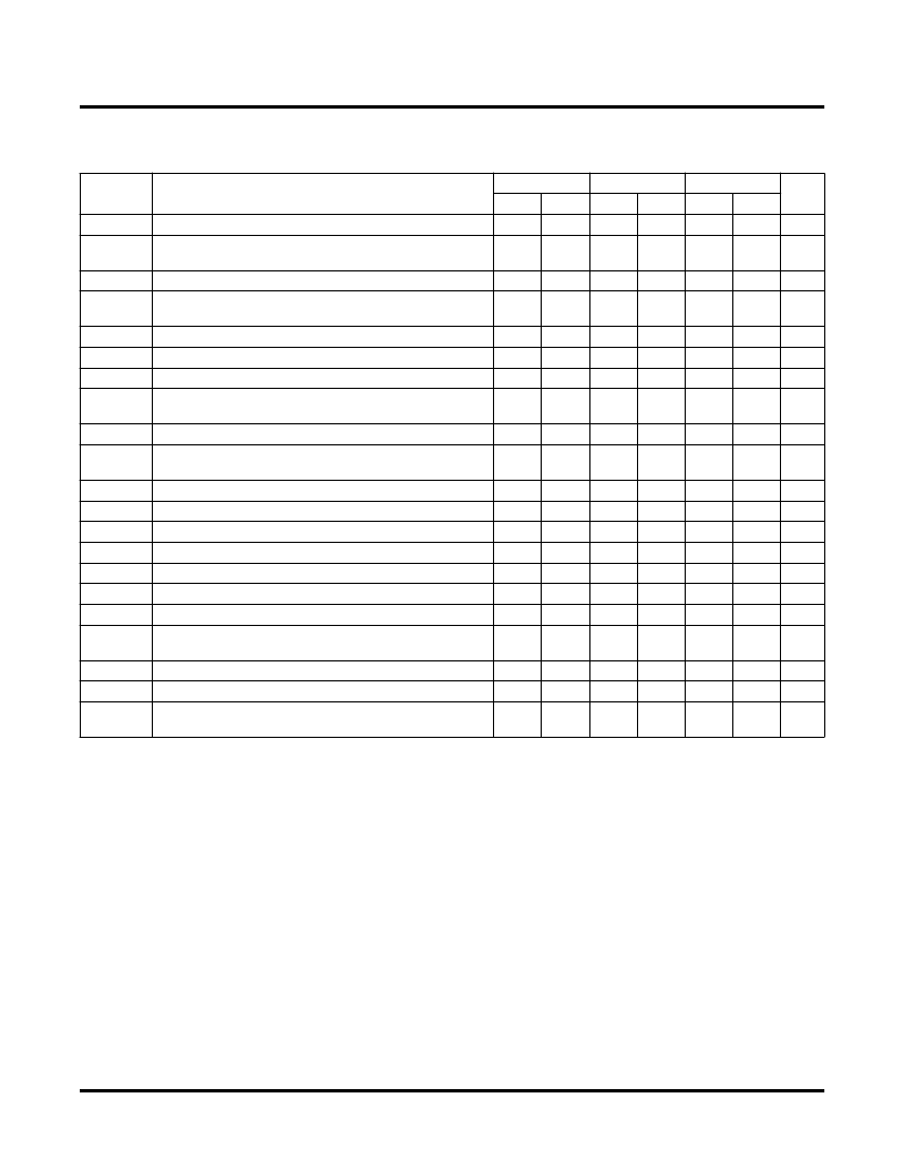
ispMACH 4000V/B/C External Switching Characteristics (Cont.)
Over Recommended Operating Conditions
Parameter
t
PD
Description
1, 2, 3
-5
-75
-10
5
Units
ns
ns
Min.
—
—
Max.
5.0
5.5
Min.
—
—
Max.
7.5
8.0
Min.
—
—
Max.
10.0
10.5
5-PT bypass combinatorial propagation delay
20-PT combinatorial propagation delay through macro-
cell
GLB register setup time before clock
GLB register setup time before clock with
T-type register
GLB register setup time before clock, input register path
GLB register setup time before clock with zero hold
GLB register hold time after clock
GLB register hold time after clock with
T-type register
GLB register hold time after clock, input register path
GLB register hold time after clock, input register path with
zero hold
GLB register clock-to-output delay
External reset pin to output delay
External reset pulse duration
Input to output local product term output enable/disable
Input to output global product term output enable/disable
Global OE input to output enable/disable
Global clock width, high or low
Global gate width low (for low transparent) or high (for
high transparent)
Input register clock width, high or low
Clock frequency with internal feedback
Clock frequency with external feedback,
[1/ (t
S
+ t
CO
)]
t
PD_MC
t
S
3.0
3.2
—
—
4.5
4.7
—
—
5.5
5.5
—
—
ns
ns
t
ST
t
SIR
t
SIRZ
t
H
1.2
2.2
0.0
0.0
—
—
—
—
1.7
2.7
0.0
0.0
—
—
—
—
1.7
2.7
0.0
0.0
—
—
—
—
ns
ns
ns
ns
t
HT
t
HIR
1.0
0.0
—
—
1.0
0.0
—
—
1.0
0.0
—
—
ns
t
HIRZ
ns
t
CO
t
R
t
RW
t
PTOE/DIS
t
GPTOE/DIS
t
GOE/DIS
t
CW
—
—
2.0
—
—
—
2.2
2.2
3.40
6.30
—
7.00
9.00
5.00
—
—
—
—
4.0
—
—
—
3.3
3.3
4.5
9.0
—
9.0
10.3
7.0
—
—
—
—
4.0
—
—
—
4.0
4.0
6.0
10.5
—
10.5
12.0
8.0
—
—
ns
ns
ns
ns
ns
ns
ns
t
GW
ns
t
WIR
f
MAX
2.2
227
156
—
—
—
3.3
168
111
—
—
—
4.0
125
86
—
—
—
ns
MHz
4
f
MAX
(Ext.)
MHz
Timing v.3.1
1. Timing numbers are based on default LVCMOS 1.8 I/O buffers. Use timing adjusters provided to calculate other standards.
2. Measured using standard switching circuit, assuming GRP loading of 1 and 1 output switching.
3. Pulse widths and clock widths less than minimum will cause unknown behavior.
4. Standard 16-bit counter using GRP feedback.
5. Only available in industrial grade.
相關(guān)PDF資料 |
PDF描述 |
|---|---|
| LC4512B-5T176C | |
| LC4512B-5T176I | |
| LC4512B-75F256C | |
| LC4512B-75F256I | |
| LC4512B-75T176C | |
相關(guān)代理商/技術(shù)參數(shù) |
參數(shù)描述 |
|---|---|
| LC4512B-5F256I1 | 制造商:LATTICE 制造商全稱:Lattice Semiconductor 功能描述:3.3V/2.5V/1.8V In-System Programmable SuperFAST High Density PLDs |
| LC4512B-5FN256C | 功能描述:CPLD - 復(fù)雜可編程邏輯器件 PROGRAMMABLE SUPER FAST HI DENSITY PLD RoHS:否 制造商:Lattice 系列: 存儲(chǔ)類型:EEPROM 大電池?cái)?shù)量:128 最大工作頻率:333 MHz 延遲時(shí)間:2.7 ns 可編程輸入/輸出端數(shù)量:64 工作電源電壓:3.3 V 最大工作溫度:+ 90 C 最小工作溫度:0 C 封裝 / 箱體:TQFP-100 |
| LC4512B-5FN256C1 | 制造商:LATTICE 制造商全稱:Lattice Semiconductor 功能描述:3.3V/2.5V/1.8V In-System Programmable SuperFAST High Density PLDs |
| LC4512B-5FN256I | 功能描述:CPLD - 復(fù)雜可編程邏輯器件 PROGRAMMABLE SUPER FAST HI DENSITY PLD RoHS:否 制造商:Lattice 系列: 存儲(chǔ)類型:EEPROM 大電池?cái)?shù)量:128 最大工作頻率:333 MHz 延遲時(shí)間:2.7 ns 可編程輸入/輸出端數(shù)量:64 工作電源電壓:3.3 V 最大工作溫度:+ 90 C 最小工作溫度:0 C 封裝 / 箱體:TQFP-100 |
| LC4512B-5FN256I1 | 制造商:LATTICE 制造商全稱:Lattice Semiconductor 功能描述:3.3V/2.5V/1.8V In-System Programmable SuperFAST High Density PLDs |
發(fā)布緊急采購,3分鐘左右您將得到回復(fù)。