- 您現在的位置:買賣IC網 > PDF目錄30732 > LC74732W ON-SCREEN DISPLAY IC, PQFP64 PDF資料下載
參數資料
| 型號: | LC74732W |
| 元件分類: | 畫面疊加 |
| 英文描述: | ON-SCREEN DISPLAY IC, PQFP64 |
| 封裝: | SQFP-64 |
| 文件頁數: | 34/38頁 |
| 文件大小: | 153K |
| 代理商: | LC74732W |
第1頁第2頁第3頁第4頁第5頁第6頁第7頁第8頁第9頁第10頁第11頁第12頁第13頁第14頁第15頁第16頁第17頁第18頁第19頁第20頁第21頁第22頁第23頁第24頁第25頁第26頁第27頁第28頁第29頁第30頁第31頁第32頁第33頁當前第34頁第35頁第36頁第37頁第38頁
No. 6527-5/38
LC74732W
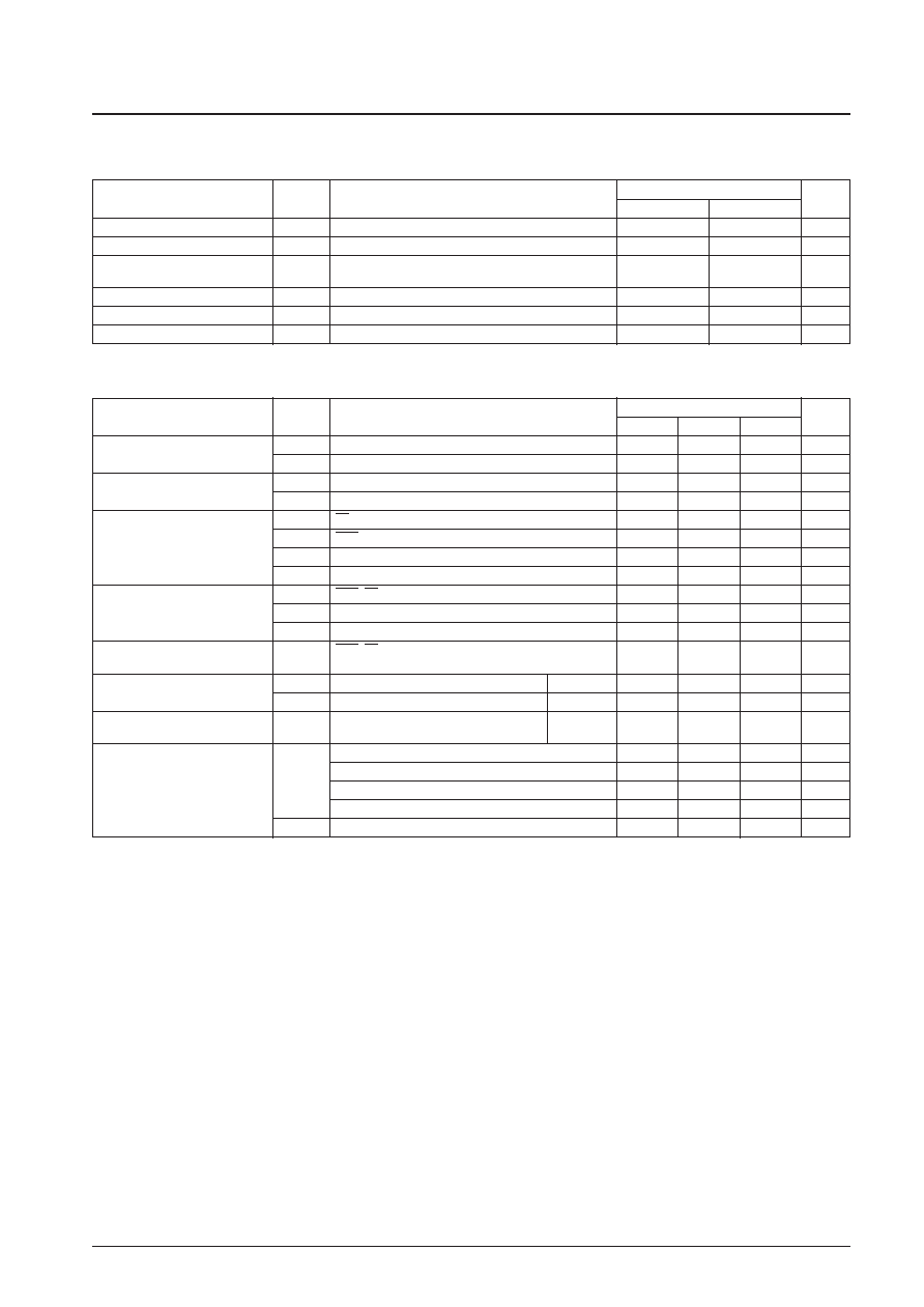
Specifications
Maximum Ratings at Ta = 25°C
Parameter
Symbol
Conditions
Ratings
Unit
min
max
Supply voltage
VDD
VDD1 and VDD2VSS – 0.3
VSS + 6.5
V
Input voltage
VIN
All input pins
VSS – 0.3
VDD1 + 0.3
V
Output voltage
VOUT
SYNCJDG, BLANK, CHARA, SEPOUT, A0 to A17,
VSS – 0.3
VDD1 + 0.3
V
CE, and OE
Allowable power dissipation
Pdmax
—
275
mW
Operating temperature
Topr
–30
+70
°C
Storage temperature
Tstg
–40
+125
°C
Parameter
Symbol
Conditions
Ratings
Unit
min
typ
max
Supply voltage
VDD1VDD1
4.5
5.0
5.5
V
VDD2VDD2
4.5
5.0
6.5
V
Supply voltage
VDD1VDD1
2.7
5.0
5.5
V
[Only for RGB output]
VDD2VDD2
2.7
5.0
6.5
V
VIH1
CS, SIN, SCLK, SEPIN, and MUTE
0.8 VDD1
—
5.5
V
High-level input voltage
VIH2
RST
0.8 VDD1
—
VDD1 + 0.3
V
VIH3
CTRL1 and OUTMOD
0.7 VDD1
—
VDD1 + 0.3
V
VIH4
D0 to D7
0.8 VDD1
—
5.5
V
VIL1
RST, CS, SIN, SCLK, SEPIN, and MUTE
VSS – 0.3
—
0.2 VDD1
V
Low-level input voltage
VIL2
CTRL1 and OUTMOD
VSS – 0.3
—
0.3 VDD1
V
VIL3
D0 to D7
VSS – 0.3
—
0.2 VDD1
V
Pull-up resistor
RPU
RST, CS, SIN, SCLK, and MUTE (when the pull-up
25
50
90
k
resistor option is specified)
Composite video signal input
VIN1
CVIN and CVCR
VDD1 = 5 V
—
2.0
—
Vp-p
voltage
VIN2
SYNIN
VDD1 = 5 V
1.5
2.0
2.5
Vp-p
Input voltage
VIN3
XtalIN (when an external clock input is used)
VDD1 = 5 V
—
5.0
Vp-p
fin = 2 fsc, 4 fsc
The XtalIN and XtalOUT oscillator pins (2 fsc: NTSC)
7.159
MHz
FOSC1
The XtalIN and XtalOUT oscillator pins (4 fsc: NTSC)
14.318
MHz
Oscillator frequency
The XtalIN and XtalOUT oscillator pins (2 fsc: PAL)
—
8.867
—
MHz
The XtalIN and XtalOUT oscillator pins (4 fsc: PAL)
—
17.734
—
MHz
FOSC2
The OSCin and OSCout oscillator pins (LC oscillator)
—
10
—
MHz
Recommended Operating Conditions
Note: If the Xtalin pin is used in clock input mode, applications must take adequate input noise prevention and reduction measures.
相關PDF資料 |
PDF描述 |
|---|---|
| LC74732W | ON-SCREEN DISPLAY IC, PQFP64 |
| LC74735NW | ON-SCREEN DISPLAY IC, PQFP80 |
| LC74735NW | ON-SCREEN DISPLAY IC, PQFP80 |
| LC74735W | ON-SCREEN DISPLAY IC, PQFP80 |
| LC74736PT | ON-SCREEN DISPLAY IC, PQFP100 |
相關代理商/技術參數 |
參數描述 |
|---|---|
| LC74732W-9811 | 制造商:SANYO Semiconductor Co Ltd 功能描述: |
| LC74732W-9811-E | 功能描述:顯示驅動器和控制器 RoHS:否 制造商:Panasonic Electronic Components 工作電源電壓:2.7 V to 5.5 V 最大工作溫度: 安裝風格:SMD/SMT 封裝 / 箱體:QFN-44 封裝:Reel |
| LC74732WH-9811-E | 功能描述:顯示驅動器和控制器 RoHS:否 制造商:Panasonic Electronic Components 工作電源電壓:2.7 V to 5.5 V 最大工作溫度: 安裝風格:SMD/SMT 封裝 / 箱體:QFN-44 封裝:Reel |
| LC74735NW | 制造商:SANYO 制造商全稱:Sanyo Semicon Device 功能描述:On-Screen Display Controller |
| LC74735NWH-8A17-E | 制造商:ON Semiconductor 功能描述: |
發布緊急采購,3分鐘左右您將得到回復。