- 您現在的位置:買賣IC網 > PDF目錄30733 > LC74761 ON-SCREEN DISPLAY IC, PDIP30 PDF資料下載
參數資料
| 型號: | LC74761 |
| 元件分類: | 畫面疊加 |
| 英文描述: | ON-SCREEN DISPLAY IC, PDIP30 |
| 封裝: | SDIP-30 |
| 文件頁數: | 6/20頁 |
| 文件大小: | 242K |
| 代理商: | LC74761 |
Second byte
Register content
DA0 to DA7
Register name
State
Function
Note
7
—
0
Second byte identification bit
6
—
0
5
—
0
4
—
0
3
MOD3
0
Normal MOD3 (P14) output (PS1 = 1)
Specifies port output data
SEL
1
Specifies MOD3 general port output
when PS1 = 0.
2
MOD2
0
Normal MOD2 (P13) output (PS1 = 1)
Specifies port output data
SEL
1
Specifies MOD2 general port output
when PS1 = 0.
1
MOD1
0
Normal MOD1 (P12) output (PS1 =1)
Specifies port output data
SEL
1
Specifies MOD1 general port output
when PS1 = 0.
0
MOD0
0
Normal MOD0 (P11) output (PS1 = 1)
Specifies port output data
SEL
1
Specifies MOD0 general port output
when PS1 = 0.
Note: When the chip is reset by the RST pin, the register states (bits) are all cleared to 0.
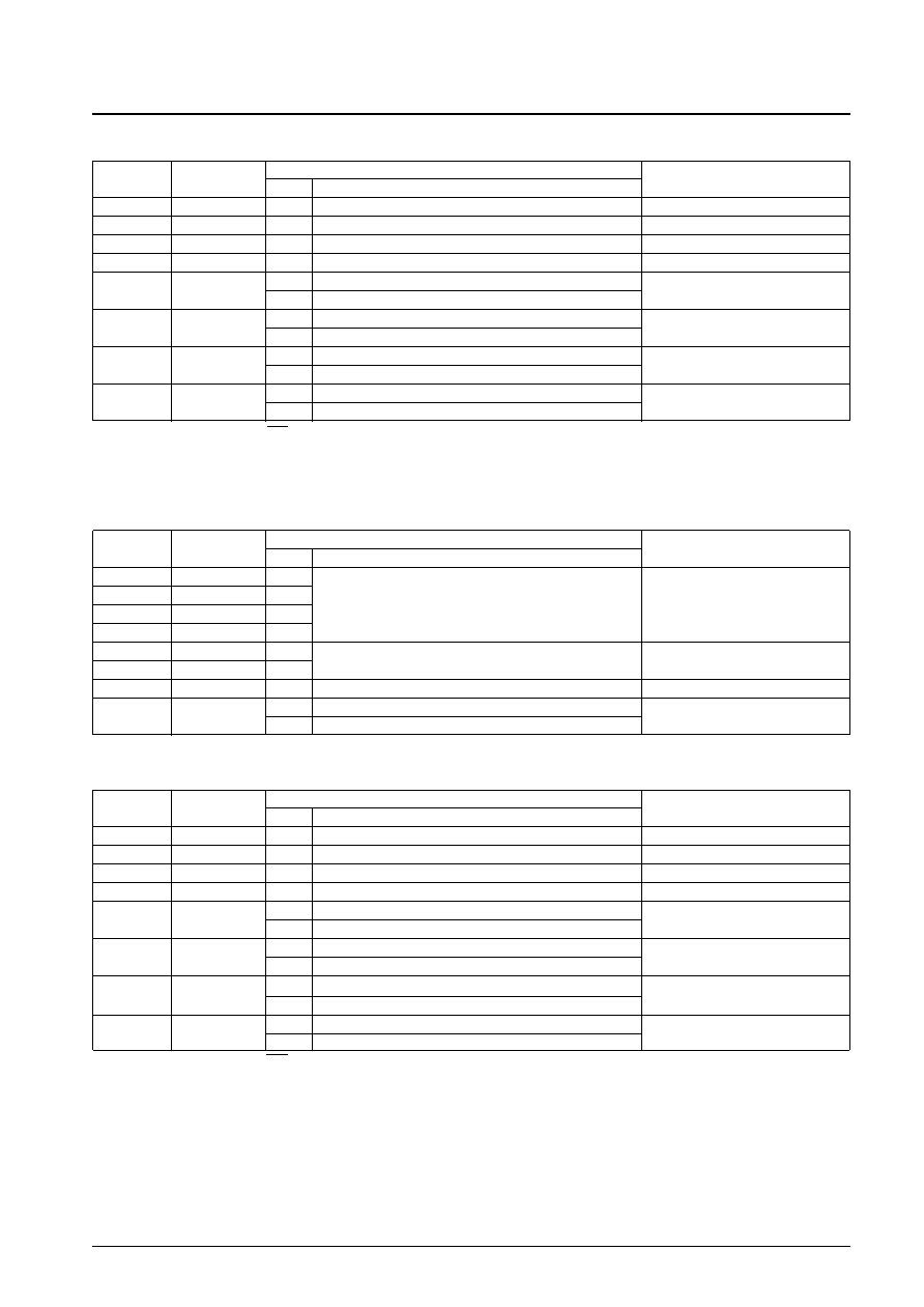
11 COMMAND73: Display Control Setting Command 7
First byte
Register content
DA0 to DA7
Register name
State
Function
Note
7
—
1
6
—
1
The command 7 identification code: sets display
5
—
1
control parameters
4
—
1
3
—
1
Expansion command 3 identification code
2
—
1
—
0
LINS
0
Selects lower 6 bits (0 to 5).
Selects lower or upper 6 bits for half
1
Selects upper 6 bits (6 to B).
tone output line setting.
Second byte
Register content
DA0 to DA7
Register name
State
Function
Note
7
—
0
Second byte identification bit
6
—
0
5
—
0
4
—
0
3
VCP
0
No feedback resistance
Specifies VCO oscillator feedback
SELECT2
1
Feedback resistance
resistance connection
2
SDETOUT
0
Normal SOUT (P29) output (PS2 = 1)
Specifies port output data
SEL
1
Specifies SOUT general port output
when PS2 = 0.
1
VOUT
0
Normal VOUT (P7) output (PS2 =1)
Specifies port output data
SEL
1
Specifies VOUT general port output
when PS2 = 0.
0
HOUT
0
Normal HOUT (P4) output (PS2 = 1)
Specifies port output data
SEL
1
Specifies HOUT general port output
when PS2 = 0.
Note: When the chip is reset by the RST pin, the register states (bits) are all cleared to 0.
No. 4846-14/20
LC74761, 74761M
相關PDF資料 |
PDF描述 |
|---|---|
| LC74761M | ON-SCREEN DISPLAY IC, PDSO30 |
| LC74761M | ON-SCREEN DISPLAY IC, PDSO30 |
| LC74761 | ON-SCREEN DISPLAY IC, PDIP30 |
| LC74763 | ON-SCREEN DISPLAY IC, PDIP30 |
| LC74763M | ON-SCREEN DISPLAY IC, PDSO30 |
相關代理商/技術參數 |
參數描述 |
|---|---|
| LC74761_11 | 制造商:SANYO 制造商全稱:Sanyo Semicon Device 功能描述:On-Screen Display LSI |
| LC74761M | 制造商:SANYO 制造商全稱:Sanyo Semicon Device 功能描述:On-Screen Display LSI |
| LC74761M-9006-E | 功能描述:顯示驅動器和控制器 RoHS:否 制造商:Panasonic Electronic Components 工作電源電壓:2.7 V to 5.5 V 最大工作溫度: 安裝風格:SMD/SMT 封裝 / 箱體:QFN-44 封裝:Reel |
| LC74763 | 制造商:SANYO 制造商全稱:Sanyo Semicon Device 功能描述:On-Screen Display LSI |
| LC74763_11 | 制造商:SANYO 制造商全稱:Sanyo Semicon Device 功能描述:On-Screen Display LSI |
發布緊急采購,3分鐘左右您將得到回復。