- 您現在的位置:買賣IC網 > PDF目錄30736 > LC80101M SPECIALTY CONSUMER CIRCUIT, PDSO28 PDF資料下載
參數資料
| 型號: | LC80101M |
| 元件分類: | 消費家電 |
| 英文描述: | SPECIALTY CONSUMER CIRCUIT, PDSO28 |
| 封裝: | MFP-28 |
| 文件頁數: | 3/9頁 |
| 文件大小: | 161K |
| 代理商: | LC80101M |
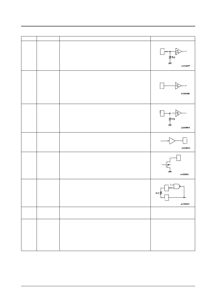
Pin Assignments and Functions
No. 5438-3/9
LC80101M
Pin No.
Pin
Function overview
Input or output circuit type
1
9
19
27
13
TEST1
TEST2
TEST3
TEST4
TESTON
Test pin 1 (Must be connected to ground or left open in normal operation.)
Test pin 2 (Must be connected to ground or left open in normal operation.)
Test pin 3 (Must be connected to ground or left open in normal operation.)
Test pin 4 (Must be connected to ground or left open in normal operation.)
Test pin (Must be connected to ground in normal operation.)
Rd: Input pin internal pull-down resistor
4
INT-R1
Inputs the output of the LC72700E pin 35.
Rd: Input pin internal pull-down resistor
5
20
21
22
23
26
DI1
BACKUP
CL2
CE2
DI2
RST2
Inputs the output of the LC72700E pin 32. An external pull-down resistor is
required. See the following page.
Input that selects normal operation when high and backup mode when low.
Clock input for the CCB serial interface
Control input for the CCB serial interface
Data input for the CCB serial interface
System reset input (negative logic)
6
7
8
25
DO1
CE1
CL1
INT-R2
Output to the LC72700E pin 31 input
Output to the LC72700E pin 30 input
Output to the LC72700E pin 29 input
Outputs an output data interrupt to the external CPU
2
3
FILCK1
FICLK2
System clock generator input
System clock generator output
Rf: External feedback resistor, 510 k
to 1.5 M (typical: 1 M)
28
14
VDD
VSS
Power supply (+4.5 to 5.5 V)
Ground connection
10, 11,
12, 15,
16, 17
18
NC
No connection pins. These pins must be left open.
24
DO2
Data output for the CCB serial interface
相關PDF資料 |
PDF描述 |
|---|---|
| LC81096 | SPEECH SYNTHESIZER, PDSO28 |
| LC81192 | SPEECH SYNTHESIZER, PDSO28 |
| LC8100 | SPEECH SYNTHESIZER, PDIP28 |
| LC82101 | SPECIALTY CONSUMER CIRCUIT, PQFP80 |
| LC82102W | SPECIALTY CONSUMER CIRCUIT, PQFP64 |
相關代理商/技術參數 |
參數描述 |
|---|---|
| LC8011-21 | 制造商:未知廠家 制造商全稱:未知廠家 功能描述:Optoelectronic |
| LC8021-21 | 制造商:未知廠家 制造商全稱:未知廠家 功能描述:Optoelectronic |
| LC8031-21 | 制造商:未知廠家 制造商全稱:未知廠家 功能描述:Optoelectronic |
| LC8041-21 | 制造商:未知廠家 制造商全稱:未知廠家 功能描述:Optoelectronic |
| LC8041R11 | 制造商:未知廠家 制造商全稱:未知廠家 功能描述:Optoelectronic |
發布緊急采購,3分鐘左右您將得到回復。