- 您現在的位置:買賣IC網 > PDF目錄377611 > LCAS6-10-L (Vicor Corporation) VI CHIP Evaluation Board PDF資料下載
參數資料
| 型號: | LCAS6-10-L |
| 廠商: | Vicor Corporation |
| 元件分類: | DC/DC變換器 |
| 英文描述: | VI CHIP Evaluation Board |
| 中文描述: | VI芯片評估板 |
| 文件頁數: | 1/4頁 |
| 文件大小: | 693K |
| 代理商: | LCAS6-10-L |
Vicor Corporation Tel: 800-735-6200 vicorpower.com
VI Chip Evaluation Board
Rev.
1.2
Page 1 - 4
4
5
if connecting to the opposite (solder) side of the board.
The VI Chip evaluation board offers a convenient means to
evaluate the performance of Vicor’s Bus Converter Modules
(BCM) or Voltage Transformation Modules (VTM).
The board has been optimized for user convenience.
Refer to the appropriate VI Chip datasheet for performance
and operating limits. The datasheets are available for
downloading at vicorpower.com.
It is important to remember that given the fast response of most
VI Chips, they can readily show the limitations of the source,
load, and associated wiring connected to the evaluation board.
Care should be exercised to minimize stray source and load
impedances in order to fully exercise the VI Chip.
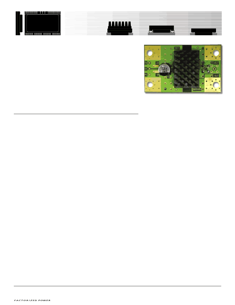
Please refer to
Figure 1
for locations of the input and output
connections as viewed from the component side. Wires may be
soldered directly to the pads in lieu of ring lugs if desired to
minimize circuit impedances.
The evaluation board should be set up as follows:
Note: Care should be taken to avoid reversing polarities
1. + IN, - IN
Connect a high quality, low noise power supply to this
location. The interconnect leads should be heavy gauge
and as short as possible. Additional capacitance may
have to be added on the evaluation board to make up
for impedances in the interconnect leads as well as
deficiencies in the source. It is important to remember
that noise from the source, as well as any input source
voltage drops, will appear at the output of the VI Chip
multiplied by its k factor.
2. + OUT, -OUT
An electronic or passive load should be connected to this
location with short heavy gauge leads. Most commercially
available electronic loads do not have current slew rates
capable of exercising the VI Chips capability. The evaluation
board can be connected directly to the application for which
the VI Chip is intended; however, the interconnect
impedances between the evaluation board and the application
can greatly effect the transient response. For applications
where transient response is critical, the user should consider
mounting the VI Chip directly to the target application PCB.
3. OUTPUT VOLTAGE MEASUREMENT JACK (J1)
This connector is provided to make an accurate
measurements of the output voltage of the VI Chip. Many
types of scope probes may be directly connected to this
point if the probe is equipped with a removable plastic
sheath. Be careful to avoid creating ground loops when
making measurements of the output or input voltage. It is
recommended that the measurements be made separately.
4. PARALLELING
The paralleling and current sharing capability of the devices
can be demonstrated by stacking multiple evaluation PCBs
and interconnecting the inputs and outputs with standoffs
of sufficient current handling capability to create a
3-dimensional array.
See Figure 3.
5. INPUT CURRENT MEASUREMENT
Acurrent probe can be passed around the +IN lead connected
to the VI Chip. Input capacitors on the evaluation board
are downstream of this measurement point.
V
I C
HIP
Evaluation Board
TM
Oscilloscope probe jack
for output voltage and
ripple measurements
Simple to use
Ring lug or solder connections
Parallelable
This board suitable for the
following VI Chip products:
Bus Converter Module (BCM)
Voltage Transformation
Module (VTM)
相關PDF資料 |
PDF描述 |
|---|---|
| LCAS6-10-L-EB | VI CHIP Evaluation Board |
| LCBG10P | Bidirectional 3.3 V I/O Transceiver for SCSI-2, SCSI-3, and SCSI-3 Fast-20 Buses( 3.3 V 雙向I/O收發器(適用于SCSI-2,SCSI-3,和SCSI-3 Fast-20 總線)) |
| LCE15 | Low Capacitance TransZorb Transient Voltage Suppressor(低電容TransZorb瞬變電壓抑制器器) |
| LCE26A | Silicon Avalanche Diodes - 1500W Axial Leaded Transient Voltage Supressors |
| LCE26 | Low Capacitance TransZorb Transient Voltage Suppressor(低電容TransZorb瞬變電壓抑制器器) |
相關代理商/技術參數 |
參數描述 |
|---|---|
| LCAS6-10-L-EB | 制造商:VICOR 制造商全稱:Vicor Corporation 功能描述:VI CHIP Evaluation Board |
| LCAS6-14F-L | 功能描述:端子 Copper Compression Lug, 1 Hole, #6 AWG, RoHS:否 制造商:AVX 產品:Junction Box - Wire to Wire 系列:9826 線規:26-18 接線柱/接頭大小: 絕緣: 顏色:Red 型式:Female 觸點電鍍:Tin over Nickel 觸點材料:Beryllium Copper, Phosphor Bronze 端接類型:Crimp |
| LCAS6-14H-L | 功能描述:端子 Copper Compression Lug, 1 Hole, #6 AWG, RoHS:否 制造商:AVX 產品:Junction Box - Wire to Wire 系列:9826 線規:26-18 接線柱/接頭大小: 絕緣: 顏色:Red 型式:Female 觸點電鍍:Tin over Nickel 觸點材料:Beryllium Copper, Phosphor Bronze 端接類型:Crimp |
| LCAS6-14-L | 功能描述:端子 6AWG 1/4" STUD RoHS:否 制造商:AVX 產品:Junction Box - Wire to Wire 系列:9826 線規:26-18 接線柱/接頭大小: 絕緣: 顏色:Red 型式:Female 觸點電鍍:Tin over Nickel 觸點材料:Beryllium Copper, Phosphor Bronze 端接類型:Crimp |
| LCAS6-38F-L | 功能描述:端子 Copper Compression Lug, 1 Hole, #6 AWG, RoHS:否 制造商:AVX 產品:Junction Box - Wire to Wire 系列:9826 線規:26-18 接線柱/接頭大小: 絕緣: 顏色:Red 型式:Female 觸點電鍍:Tin over Nickel 觸點材料:Beryllium Copper, Phosphor Bronze 端接類型:Crimp |
發布緊急采購,3分鐘左右您將得到回復。