- 您現在的位置:買賣IC網 > PDF目錄367544 > LE79R251JC Telecommunication IC PDF資料下載
參數資料
| 型號: | LE79R251JC |
| 英文描述: | Telecommunication IC |
| 中文描述: | 通信集成電路 |
| 文件頁數: | 8/22頁 |
| 文件大小: | 533K |
| 代理商: | LE79R251JC |
P R E L I M I N A R Y
8
Le79R251 ISLIC Data Sheet
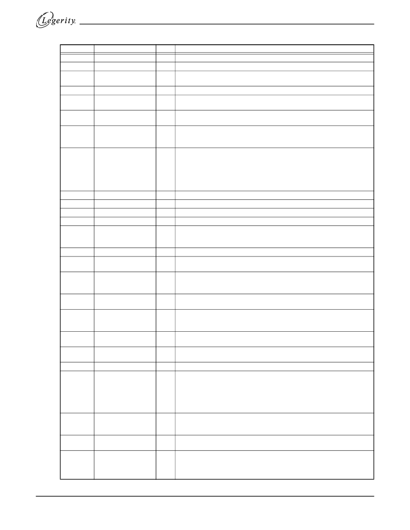
PIN DESCRIPTIONS
Pin
Pin Name
I/O
Description
AD, BD
A, B Line Drivers
O
Provide the currents to the A and B leads of the subscriber loop.
BGND
Ground
Ground return for high and low battery supplies.
CREF
+3.3 VDC
VCCD reference. It is the digital high logic supply rail, used by the ISLIC to ISLAC
interface.
GND
Ground
Analog and digital ground return for VCC.
HPA, HPB
High-Pass Filter
Capacitor
O
These pins connect to CHP, the external high-pass filter capacitor that separates
the DC loop-voltage from the voice transmission path.
ILG
Longitudinal Current
Sense
O
ILG is proportional to the common-mode line current (IAD – IBD), except in
disconnect mode, where ILG is proportional to the current into grounded SB.
IMT
Metallic Current Sense
O
IMT is proportional to the differential line current (IAD + IBD), except in disconnect
mode, where IMT is proportional to the current into grounded SA.The Le79R251
device indicates thermal overload by pulling IMT to >2.8 V.
LD
Register Load
I
The LD pin controls the input latch and responds to a 3-level input. When the LD
pin is a logic 1 (CREF - 1), the logic levels on P1–P3 latch into the Le79R251
device control register bits that operate the mode-decoder. When the LD pin is a
logic 0 (< 0.6 V), the logic levels on P1–P3 latch into the Le79R251 device control
register bits that control the relay drivers (RD1–RD3). When the LD pin level is at
~V
REF
± 0.3 V the control register contents are locked.
Inputs to the latch for the operating-mode decoder and the relay-drivers.
P1–P3
Control Bus
I
R1
Relay 1 Driver
O
Collector connection for relay 1 driver. Emitter internally connected to BGND.
R2
Relay 2 Driver
O
Collector connection for relay 2 driver. Emitter internally connected to RYE
R3
Relay 3 Driver
O
Collector connection for relay 3 driver. Emitter internally connected to RYE.
RSN
Receive Summing
Node
I
The metallic current between AD and BD is equal to 500 times the current into this
pin. Networks that program receive gain and two-wire impedance connect to this
node. This input is at a virtual potential of VREF.
RSVD
Reserved
This is used during Legerity testing. In the application, this pin must be left floating.
RYE
Relay 2, 3 Common
Emitter
O
Emitter connection for R2 and R3. Normally connected to relay ground.
SA, SB
A, B Lead Voltage
Sense
I
Sense the voltages on the line side of the fuse resistors at the A and B leads.
External sense resistors, RSA and RSB, protect these pins from lightning or
power-cross.
TMP, TMN,
TMS
Thermal Management
External resistors connected from TMP to TMS and TMN to VBL to offload excess
power
from the Le79R251 device.
VBH
Battery (Power)
Connection to high-battery supply used for ringing and long loops. Connects to the
substrate. When only a single negative battery is available, it connects to both
VBH and VBL.
VBL
Battery (Power)
Connection to low-battery supply used for short loops. When only a single negative
battery is available, this pin must be connected to VBH.
VBP
Positive Battery
(Power)
Used in Ringing State and for Extended Loop operation.
VCC
+5 V Power Supply
Positive supply for low voltage analog and digital circuits in the Le79R251 device.
VLB
Longitudinal Voltage
I
Sets the DC longitudinal voltage of the Le79R251 device. It is the reference for the
longitudinal control loop. When the VLB pin is greater than VREF, the Le79R251
device sets the longitudinal voltage to a voltage approximately half-way between
the positive and negative power supply battery rails. When the VLB pin is driven
to levels between 0V and VREF, the longitudinal voltage decreases linearly with
the voltage on the VLB pin.
VREF
1.4 V Analog
Reference
I
The ISLAC chip provides this voltage which is used by the Le79R251 device for
internal reference purposes. All analog input and output signals interfacing to the
ISLAC chip are referenced to this pin.
VSAB
Loop Voltage
O
Scaled-down version of the voltage between the sense points SA and SB on this
pin.
VTX
4-Wire Transmit Signal
O
The voltage between this pin and VREF is a scaled down version of the AC
component of the voltage sensed between the SA and SB pins. One end of the
two-wire input impedance programming network connects to VTX. The voltage at
VTX swings positive and negative with respect to VREF.
相關PDF資料 |
PDF描述 |
|---|---|
| LEA20033 | ASIC |
| LEA20040 | ASIC |
| LEA20046 | ASIC |
| LEA20056 | ASIC |
| LEA20066 | ASIC |
相關代理商/技術參數 |
參數描述 |
|---|---|
| LE79R70-1DJC | 制造商:Microsemi Corporation 功能描述:SLIC 1CH 40DB 110MA 5V 32PLCC - Rail/Tube 制造商:MICROSEMI CONSUMER MEDICAL PRODUCT GROUP 功能描述:IC SLIC 1CH 40DB LGBAL 32PLCC |
| LE79R70-1DJCT | 制造商:Microsemi Corporation 功能描述:1CH SLIC 40DB LGBAL P RV PL32TR 制造商:Microsemi Corporation 功能描述:SLIC 1CH 40DB 110MA 5V 32PLCC - Tape and Reel 制造商:MICROSEMI CONSUMER MEDICAL PRODUCT GROUP 功能描述:IC SLIC 1CH 40DB LGBAL 32PLCC 制造商:Microsemi Corporation 功能描述:IC SLIC 1CH 40DB LGBAL 32PLCC |
| LE79R70-1FQC | 制造商:Microsemi Corporation 功能描述:SLIC 1CH 40DB 110MA 5V 32QFN EP - Trays 制造商:Microsemi Corporation 功能描述:SINGLE SLIC SHORT LOOP LONG-BAL POL REV 制造商:Zarlink Semiconductor Inc 功能描述:SINGLE SLIC SHORT LOOP LONG-BAL POL REV |
| LE79R70-1FQCT | 制造商:Microsemi Corporation 功能描述:SLIC 1CH 40DB 110MA 5V 32QFN EP - Tape and Reel |
| LE79R70DJC | 制造商:Microsemi Corporation 功能描述:SLIC 1CH 40DB 110MA 5V 32PLCC - Rail/Tube 制造商:MICROSEMI CONSUMER MEDICAL PRODUCT GROUP 功能描述:IC SLIC 1CH 40DB LGBAL 32PLCC 制造商:Microsemi Corporation 功能描述:IC SLIC 1CH 40DB LGBAL 32PLCC |
發布緊急采購,3分鐘左右您將得到回復。