- 您現(xiàn)在的位置:買(mǎi)賣(mài)IC網(wǎng) > PDF目錄361022 > LF353 (意法半導(dǎo)體) WIDE BANDWIDTH DUAL J-FET OPERATIONAL AMPLIFIERS PDF資料下載
參數(shù)資料
| 型號(hào): | LF353 |
| 廠商: | 意法半導(dǎo)體 |
| 英文描述: | WIDE BANDWIDTH DUAL J-FET OPERATIONAL AMPLIFIERS |
| 中文描述: | 寬帶雙的J - FET的運(yùn)算放大器 |
| 文件頁(yè)數(shù): | 2/14頁(yè) |
| 文件大小: | 597K |
| 代理商: | LF353 |
第1頁(yè)當(dāng)前第2頁(yè)第3頁(yè)第4頁(yè)第5頁(yè)第6頁(yè)第7頁(yè)第8頁(yè)第9頁(yè)第10頁(yè)第11頁(yè)第12頁(yè)第13頁(yè)第14頁(yè)
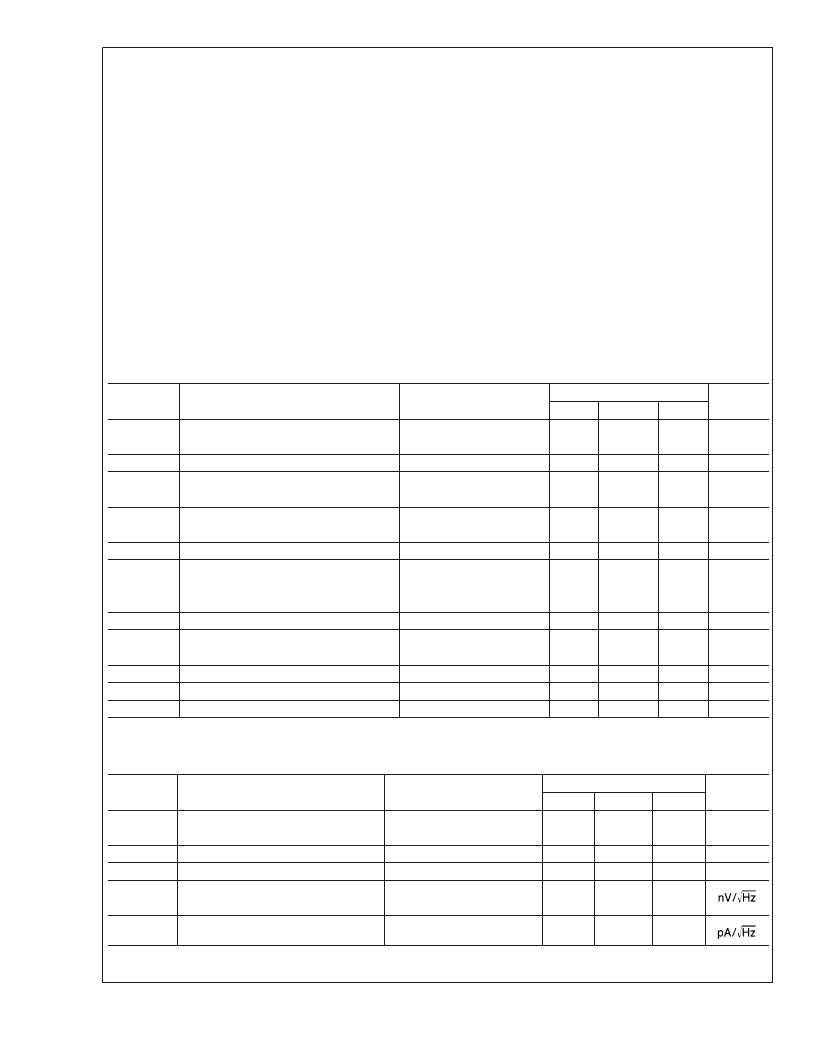
Absolute Maximum Ratings
(Note 1)
If Military/Aerospace specified devices are required,
please contact the National Semiconductor Sales Office/
Distributors for availability and specifications.
Supply Voltage
Power Dissipation
Operating Temperature Range
T
j
(MAX)
Differential Input Voltage
Input Voltage Range (Note 3)
Output Short Circuit Duration
Storage Temperature Range
Lead Temp. (Soldering, 10 sec.)
Soldering Information
Dual-In-Line Package
Soldering (10 sec.)
±
18V
(Note 2)
0C to +70C
150C
±
30V
±
15V
Continuous
65C to +150C
260C
260C
Small Outline Package
Vapor Phase (60 sec.)
Infrared (15 sec.)
See AN-450 “Surface Mounting Methods and Their Effect
on Product Reliability” for other methods of soldering
surface mount devices.
ESD Tolerance (Note 8)
θ
JA
M Package
215C
220C
1000V
TBD
Note 1:
Absolute Maximum Ratings indicate limits beyond which damage to
the device may occur. Operating ratings indicate conditions for which the
device is functional, but do not guarantee specific performance limits. Elec-
trical Characteristics state DC and AC electrical specifications under particu-
lar test conditions which guarantee specific performance limits. This assumes
that the device is within the Operating Ratings. Specifications are not guar-
anteed for parameters where no limit is given, however, the typical value is a
good indication of device performance.
DC Electrical Characteristics
(Note 5)
Symbol
Parameter
Conditions
LF353
Typ
5
Units
MIn
Max
10
13
V
OS
Input Offset Voltage
R
S
=10k
, T
A
=25C
Over Temperature
R
S
=10 k
T
j
=25C, (Notes 5, 6)
T
j
≤
70C
T
j
=25C, (Notes 5, 6)
T
j
≤
70C
T
j
=25C
V
S
=
±
15V, T
A
=25C
V
O
=
±
10V, R
L
=2 k
Over Temperature
V
S
=
±
15V, R
L
=10k
V
S
=
±
15V
mV
mV
μV/C
pA
nA
pA
nA
V/mV
V
OS
/
T
I
OS
Average TC of Input Offset Voltage
Input Offset Current
10
25
100
4
200
8
I
B
Input Bias Current
50
R
IN
A
VOL
Input Resistance
Large Signal Voltage Gain
10
12
100
25
15
±
12
±
11
V/mV
V
V
V
dB
dB
mA
V
O
V
CM
Output Voltage Swing
Input Common-Mode Voltage
Range
Common-Mode Rejection Ratio
Supply Voltage Rejection Ratio
Supply Current
±
13.5
+15
12
100
100
3.6
CMRR
PSRR
I
S
R
S
≤
10k
(Note 7)
70
70
6.5
AC Electrical Characteristics
(Note 5)
Symbol
Parameter
Conditions
LF353
Typ
120
Units
Min
Max
Amplifier to Amplifier Coupling
T
A
=25C, f=1 Hz20 kHz
(Input Referred)
V
S
=
±
15V, T
A
=25C
V
S
=
±
15V, T
A
=25C
T
A
=25C, R
S
=100
,
f=1000 Hz
T
j
=25C, f=1000 Hz
dB
SR
GBW
e
n
Slew Rate
Gain Bandwidth Product
Equivalent Input Noise Voltage
8.0
2.7
13
4
16
V/μs
MHz
i
n
Equivalent Input Noise Current
0.01
L
www.national.com
2
相關(guān)PDF資料 |
PDF描述 |
|---|---|
| LF353 | Wide Bandwidth Dual JFET Input Operational Amplifier |
| LF353H | Wide Bandwidth Dual JFET Input Operational Amplifier |
| LF353M | Wide Bandwidth Dual JFET Input Operational Amplifier |
| LF353N | Wide Bandwidth Dual JFET Input Operational Amplifier |
| LF353 | Amplifiers and Comparators |
相關(guān)代理商/技術(shù)參數(shù) |
參數(shù)描述 |
|---|---|
| LF353AD | 制造商:未知廠家 制造商全稱(chēng):未知廠家 功能描述:Voltage-Feedback Operational Amplifier |
| LF353AN | 制造商:未知廠家 制造商全稱(chēng):未知廠家 功能描述:Voltage-Feedback Operational Amplifier |
| LF353BD | 制造商:未知廠家 制造商全稱(chēng):未知廠家 功能描述:Voltage-Feedback Operational Amplifier |
| LF353BN | 制造商:未知廠家 制造商全稱(chēng):未知廠家 功能描述:Voltage-Feedback Operational Amplifier |
| LF353D | 功能描述:運(yùn)算放大器 - 運(yùn)放 Op Amp RoHS:否 制造商:STMicroelectronics 通道數(shù)量:4 共模抑制比(最小值):63 dB 輸入補(bǔ)償電壓:1 mV 輸入偏流(最大值):10 pA 工作電源電壓:2.7 V to 5.5 V 安裝風(fēng)格:SMD/SMT 封裝 / 箱體:QFN-16 轉(zhuǎn)換速度:0.89 V/us 關(guān)閉:No 輸出電流:55 mA 最大工作溫度:+ 125 C 封裝:Reel |
發(fā)布緊急采購(gòu),3分鐘左右您將得到回復(fù)。