- 您現在的位置:買賣IC網 > PDF目錄377624 > LF9502JC20 (LOGIC DEVICES INC) 2K Programmable Line Buffer PDF資料下載
參數資料
| 型號: | LF9502JC20 |
| 廠商: | LOGIC DEVICES INC |
| 元件分類: | 數字信號處理外設 |
| 英文描述: | 2K Programmable Line Buffer |
| 中文描述: | 10-BIT, DSP-PIPELINE REGISTER, PQCC44 |
| 封裝: | PLASTIC, LCC-44 |
| 文件頁數: | 1/7頁 |
| 文件大小: | 52K |
| 代理商: | LF9502JC20 |
DEVICES INCORPORATED
1
LF9502
2K Programmable Line Buffer
2K Programmable Line Buffer
08/16/2000–LDS.9502-G
Video Imaging Products
K
50 MHz Maximum Operating
Frequency
K
Programmable Buffer Length from
2 to 2049 Clock Cycles
K
10-bit Data Inputs and Outputs
K
Data Delay and Data Recirculation
Modes
K
Supports Positive or Negative Edge
System Clocks
K
Expandable Data Word Width or
Buffer Length
K
44-pin PLCC, J-Lead
FEATURES
DESCRIPTION
DEVICES INCORPORATED
The
LF9502
is a high-speed, 10-bit
programmable line buffer. Some
applications the LF9502 is useful for
include sample rate conversion, data
time compression/ expansion, soft-
ware controlled data alignment, and
programmable serial data shifting. By
using the MODSEL pin, two different
modes of operation can be selected:
delay mode and data recirculation
mode. The delay mode provides a
minimum of 2 to a maximum of 2049
clock cycles of delay between the
input and output of the device. The
data recirculation mode provides a
feedback path from the data output to
the data input for use as a program-
mable circular buffer.
By using the length control input
(LC
10-0
) and the length control enable
(LCEN) the length of the delay buffer
or amount of recirculation delay can
be programmed. Providing a delay
value on the LC
10-0
inputs and driving
LCEN LOW will load the delay value
into the length control register on the
next selected clock edge. Two regis-
ters, one preceeding the program-
mable delay RAM and one following,
are included in the delay path. There-
fore, the programmed delay value
should equal the desired delay minus
2. This consequently means that the
value loaded into the length control
register must range from 0 to 2047 (to
provide an overall range of 2 to 2049).
The active edge of the clock input,
either positive or negative edge, can
be selected with the clock select
(CLKSEL) input. All timing is based
on the active clock edge selected by
CLKSEL. Data can be held tempo-
rarily by using the clock enable
(CLKEN) input.
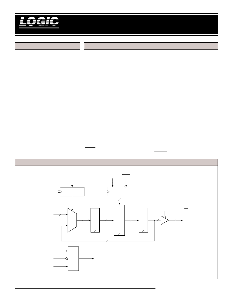
LF9502 B
LOCK
D
IAGRAM
R
M
P
2
R
DI
9-0
10
10
10
10
10
10
10
MODSEL
C
G
CLKSEL
CLKEN
CLK
OE
REGISTER
LCO
10-0
LCEN
11
11
TO ALL REGISTERS
REGISTER
DO
9-0
相關PDF資料 |
PDF描述 |
|---|---|
| LF9502JC25 | 2K Programmable Line Buffer |
| LFCN-1000 | Low Pass Filter |
| LFCN-1000D | Low Pass Filter |
| LFCN-105 | Ceramic Low Pass Filter |
| LFCN-105D | Ceramic Low Pass Filter |
相關代理商/技術參數 |
參數描述 |
|---|---|
| LF9502JC25 | 制造商:LOGIC 制造商全稱:LOGIC 功能描述:2K Programmable Line Buffer |
| LF9502JC31 | 制造商:未知廠家 制造商全稱:未知廠家 功能描述:x10 Synchronous FIFO |
| LF9502JC40 | 制造商:未知廠家 制造商全稱:未知廠家 功能描述:x10 Synchronous FIFO |
| LF99151MF8B | 制造商:Texas Instruments 功能描述: |
| LF99151Z | 制造商:Texas Instruments 功能描述: |
發布緊急采購,3分鐘左右您將得到回復。