- 您現(xiàn)在的位置:買賣IC網(wǎng) > PDF目錄367549 > LG1625AXF (Lineage Power) Laser Driver(激光驅(qū)動器) PDF資料下載
參數(shù)資料
| 型號: | LG1625AXF |
| 廠商: | Lineage Power |
| 英文描述: | Laser Driver(激光驅(qū)動器) |
| 中文描述: | 激光驅(qū)動器(激光驅(qū)動器) |
| 文件頁數(shù): | 3/12頁 |
| 文件大小: | 363K |
| 代理商: | LG1625AXF |
Lucent Technologies Inc.
3
Data Sheet
June 1999
LG1625AXF Laser Driver
Pin Information
(continued)
Absolute Maximum Ratings
Stresses in excess of the absolute maximum ratings can cause permanent or latent damage to the device. These
are absolute stress ratings only. Functional operation of the device is not implied at these or any other conditions in
excess of those given in the operational sections of this device specification. Exposure to absolute maximum rat-
ings for extended periods can adversely affect device reliability.
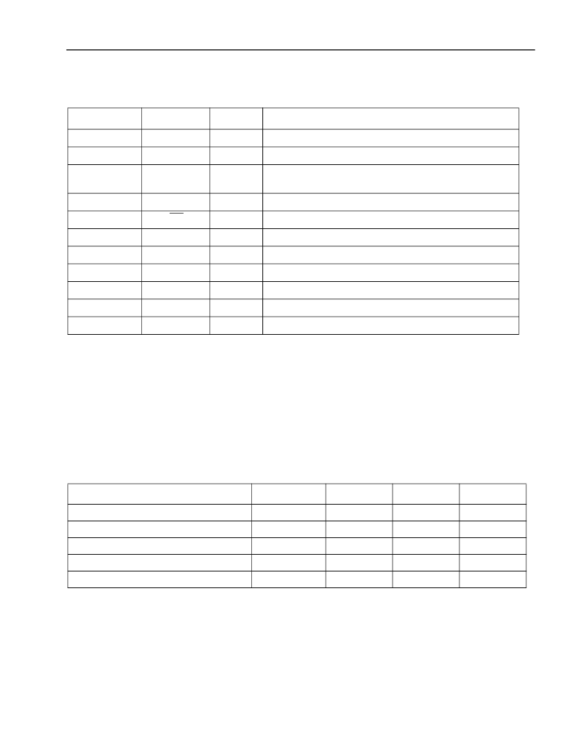
Table 1. LG1625AXF Pin Description
Pin
Symbol
Type
*
* I = input, O = output, P = power.
Connection to V
TH
for threshold adjustment should be made through pin 24. Pin 7 is made available for additional bypassing of V
TH
(See
Figure 5 on page 6, Typical Test Circuit).
Name/Definition
1, 6, 13, 22, 23
V
SS1
P
V
SS1
Supply.
–5.2 V power supply pin.
2
V
IN
I
Data Input.
3, 4, 5, 8, 9, 10,
14, 15, 17
GND
P
Ground.
7, 24
V
TH
I
Threshold Control.
Input (eye crossing).
11
MK
O
Complementary Mark Density Output.
12
MK
O
Mark Density Output.
16
I
OUT
O
Output.
dc couple to laser cathode.
18
V
PRE
I
Prebias Control Input.
19
V
SS2
P
V
SS2
.
–5.2 V supply for output prebias.
20
V
SS3
P
V
SS3
.
–5.2 V supply for output modulation.
21
V
MOD
I
Modulation Current Control Input.
Table 2. Absolute Maximum Ratings
(at T
A
= 25 °C unless otherwise specified)
Parameter
Symbol
Min
Max
Unit
Supply Voltage
V
SS
—
–5.95
V
°
C
°
C
Storage Temperature
T
stg
–40
125
Operating Case Temperature Range
T
C
0
75
Input Voltage
V
I
GND
V
SS
V
Power Dissipation
P
D
—
1
W
相關PDF資料 |
PDF描述 |
|---|---|
| LG5360JM | Optoelectronic |
| LS5360KN | Optoelectronic |
| LGK380E7500 | Optoelectronic |
| LSK382P | Optoelectronic |
| LYK380E7500 | Optoelectronic |
相關代理商/技術參數(shù) |
參數(shù)描述 |
|---|---|
| LG1626DXC | 制造商:AGERE 制造商全稱:AGERE 功能描述:LG1626DXC Modulator Driver |
| LG1627BXC | 制造商:AGERE 制造商全稱:AGERE 功能描述:LG1627BXC Clocked Laser Driver |
| LG1628AXA | 制造商:AGERE 制造商全稱:AGERE 功能描述:LG1628AXA SONET/SDH 2.488 Gbits/s Transimpedance Amplifier |
| LG-170-8SEF-CT | 制造商:LIGITEK 制造商全稱:LIGITEK electronics co., ltd. 功能描述:LED SMD |
| LG-170-8UG-CT | 制造商:LIGITEK 制造商全稱:LIGITEK electronics co., ltd. 功能描述:LED SMD |
發(fā)布緊急采購,3分鐘左右您將得到回復。