- 您現在的位置:買賣IC網 > PDF目錄361023 > LM1042 (NATIONAL SEMICONDUCTOR CORP) Fluid Level Detector PDF資料下載
參數資料
| 型號: | LM1042 |
| 廠商: | NATIONAL SEMICONDUCTOR CORP |
| 元件分類: | 模擬信號調理 |
| 英文描述: | Fluid Level Detector |
| 中文描述: | SPECIALTY ANALOG CIRCUIT, PDIP16 |
| 文件頁數: | 2/8頁 |
| 文件大小: | 170K |
| 代理商: | LM1042 |
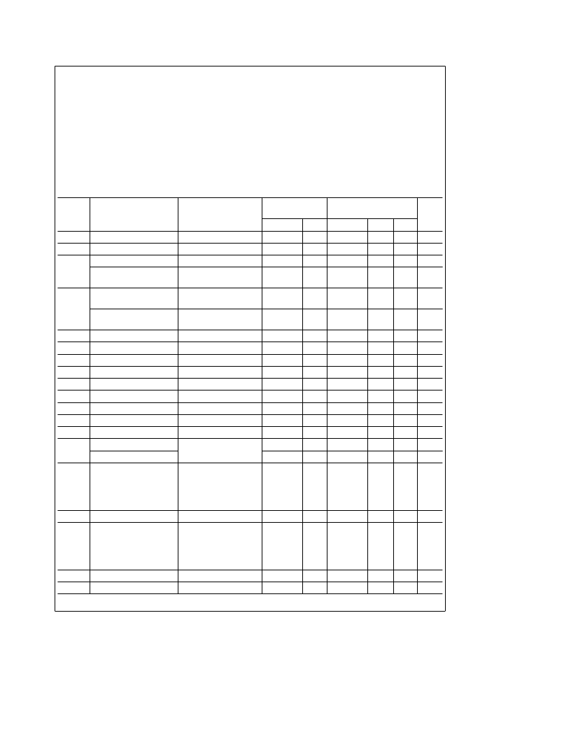
Absolute Maximum Ratings
If Military/Aerospace specified devices are required,
please contact the National Semiconductor Sales
Office/Distributors for availability and specifications.
Supply Voltage V
CC
Voltage at Pin 8
32V
32V
Positive Peak Voltage (Pins 6, 8, 3) (Note 1)
10 ms 2A
50V
Output Current Pin 4, (I
4
)(sink)
10 mA
Output Current Pin 11 (source)
25 mA
Output Current Pin 16
g
10 mA
Operating Temperature Range
b
40
§
C to
a
80
§
C
b
55
§
C to
a
150
§
C
Storage Temperature Range
Lead Temperature (Soldering 10 sec.)
260
§
C
Package Power Dissipation
T
A
e
25
§
C (Note 8)
Device Power Dissipation
1.8W
0.9W
Electrical Characteristics
V
CC
e
13V, T
A
within operating range except where stated otherwise. C
T
e
22
m
F, R
T
e
12k
Tested Limits
(Note 2)
Design Limits
(Note 3)
Symbol
Parameter
Conditions
Units
Min
Max
Min
Typ
Max
V
CC
Supply Voltage
7.5
18
7.5
13
18
V
I
S
Supply Current
35
35
mA
V
REG
Regulated Voltage
Pins 15 and 11 connected
5.7
6.15
5.65
5.9
6.2
V
Stability Over V
CC
Range
Referred to value at
V
CC
e
13V (Note 4)
g
0.5
g
0.5
%
V
6
–V
3
Probe Current
Reference Voltage
2.15
2.35
2.10
2.25
2.40
V
Probe Current Regulation
Over V
CC
Range
(Note 4)
g
0.5
g
0.8
%
T
1
Ramp Timing
SeeFigure 5
20
37
15
31
42
ms
T
2
–T
1
3
16
ms
T
4
–T
1
Ramp Timing
1.4
2.1
1.4
1.75
2.1
s
T
STAB
Ramp Timing Stability
Over V
CC
Range
a
5
g
5
%
R
T
Ramp Resistor Range
3
15
3
15.0
k
X
V
8
Start Input Logic High Level
1.7
1.7
V
V
8
Start Input Logic Low Level
0.5
0.5
V
I
8
Start Input Current
V
8
e
V
CC
100
100
nA
I
8
Start Input Current
V
8
e
0V
300
300
nA
V
16
Maximum Output Voltage
R
L
e
600
X
from
Pin 16 to V
REG
V
REG
b
0.3
V
REG
b
0.3
V
Minimum Output Voltage
0.5
0.2
0.6
V
PROBE 1
Probe 1 Gain
G
1
Pin 1 80 mV to 520 mV
(Notes 6, 7)
Pin 1 80 mV to 520 mV
(Note 7)
9.9
10.4
10.15
Non-linearity of G
1
b
1
a
1
b
2
0
2
%
OS
1
Pin 1 Offset
(Note 7)
g
5
mV
PROBE 2
Probe 2 Gain
G
2
Pin 7 240 mV to 1.562V
(Note 7)
Pin 7 240 mV to 1.562V
(Note 7)
3.31
3.49
3.4
Non-linearity of G
2
b
1
a
1
b
2
0.2
2
%
OS
7
Pin 7 Offset
(Note 7)
g
5
mV
R
7
Input impedance
5
M
X
2
相關PDF資料 |
PDF描述 |
|---|---|
| LM1042N | Fluid Level Detector |
| LM104 | Negative Regulator |
| LM304 | Negative Regulator |
| LM204 | Negative Regulator |
| LM204H | Negative Regulator |
相關代理商/技術參數 |
參數描述 |
|---|---|
| LM104-204-304 | 制造商:未知廠家 制造商全稱:未知廠家 功能描述:曾流調整器扣用于很多其他控制虛用 |
| LM1042N | 制造商:NSC 制造商全稱:National Semiconductor 功能描述:Fluid Level Detector |
| LM1042N/A+ | 制造商:未知廠家 制造商全稱:未知廠家 功能描述:FLUID DETECTOR|BIPOLAR|DIP|16PIN|PLASTIC |
| LM1042N/B+ | 制造商:未知廠家 制造商全稱:未知廠家 功能描述:FLUID DETECTOR|BIPOLAR|DIP|16PIN|PLASTIC |
| LM1044 | 制造商:NSC 制造商全稱:National Semiconductor 功能描述:Analog Video Switch |
發布緊急采購,3分鐘左右您將得到回復。