- 您現在的位置:買賣IC網 > PDF目錄361025 > LM2622 PDF資料下載
參數資料
| 型號: | LM2622 |
| 文件頁數: | 6/10頁 |
| 文件大小: | 254K |
| 代理商: | LM2622 |
Detailed Description
(Continued)
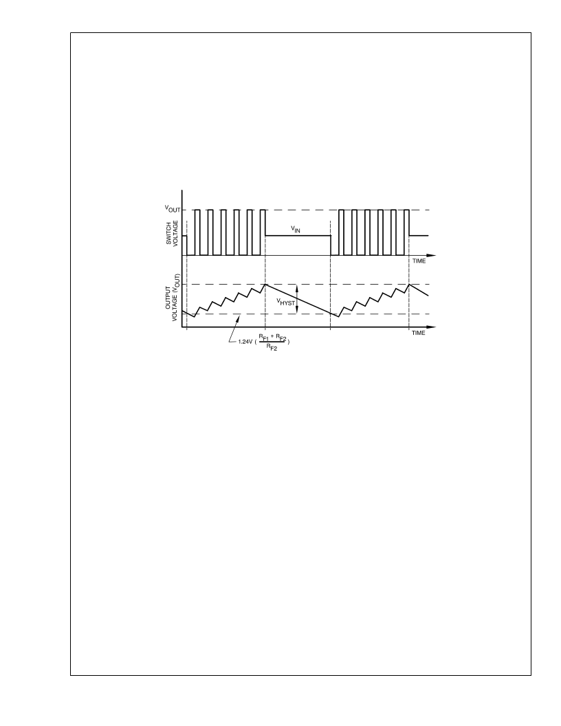
This control scheme uses a hysteresis window to regulate
the output voltage. When the output voltage is below the up-
per threshold of the window, the LM2621 switches continu-
ously with a fixed duty cycle of 70% at the switching fre-
quency selected by the user. During the first part of each
switching cycle, the internal N-channel MOSFET switch is
turned on. This causes the current to ramp up in the inductor
and store energy. During the second part of each switching
cycle, the MOSFET is turned off. The voltage across the in-
ductor reverses and forces current through the diode to the
output filter capacitor and the load. Thus when the LM2621
switches continuously, the output voltage starts to ramp up.
When the output voltage hits the upper threshold of the win-
dow, the LM2621 stops switching completely. This causes
the output voltage to droop because the energy stored in the
output capacitor is depleted by the load. When the output
voltage hits the lower threshold of the hysteresis window, the
LM2621 starts switching continuously again causing the out-
put voltage to ramp up towards the upper threshold. Figure 2
shows the switch voltage and output voltage waveforms.
Because of this type of control scheme, the quiescent cur-
rent is inherently very low. At light loads the gated oscillator
control scheme offers a much higher efficiency compared to
the conventional PWM control scheme.
LOW VOLTAGE START-UP
The LM2621 can start-up from input voltages as low as 1.1V.
On start-up, the control circuitry switches the N-channel
MOSFET continuously at 70% duty cycle until the output
voltage reaches 2.5V. After this output voltage is reached,
the normal step-up regulator feedback and gated oscillator
control scheme take over. Once the device is in regulation it
can operate down to a 0.65V input, since the internal power
for the IC can be boot-strapped from the output using the
V
DD
pin.
SHUTDOWN
The LM2621 features a shutdown mode that reduces the
quiescent current to less than a guaranteed 2.5μA over tem-
perature. This extends the life of the battery in battery pow-
ered applications. During shutdown, all feedback and control
circuitry is turned off. The regulator’s output voltage drops to
one diode drop below the input voltage. Entry into the shut-
down mode is controlled by the active-low logic input pin EN
(Pin 2). When the logic input to this pin pulled below
0.15V
, the device goes into shutdown mode. The logic in-
put to this pin should be above 0.7V
DD
for the device to work
in normal step-up mode.
OUTPUT VOLTAGE RIPPLE FREQUENCY
A major component of the output voltage ripple is due to the
hysteresis used in the gated oscillator control scheme. The
frequency of this voltage ripple is proportional to the load
current. The frequency of this ripple does not necessitate the
use of larger inductors and capacitors however, since the
size of these components is determined by the switching fre-
quency of the oscillator which can be set upto 2MHz using
an external resistor.
INTERNAL CURRENT LIMIT AND THERMAL
PROTECTION
An internal cycle-by-cycle current limit serves as a protection
feature. This is set high enough (2.85A typical, approxi-
mately 4A maximum) so as not to come into effect during
normal operating conditions. An internal thermal protection
circuitry disables the MOSFET power switch when the junc-
tion temperature (T
J
) exceeds about 160C. The switch is
re-enabled when T
J
drops below approximately 135C.
Design Procedure
SETTING THE OUTPUT VOLTAGE
The output voltage of the step-up regulator can be set be-
tween 1.24V and 14V by connecting a feedback resistive di-
vider made of R
F1
and R
F2
. The resistor values are selected
as follows:
R
F2
= R
F1
/[(V
OUT
/ 1.24) 1]
A value of 150k
is suggested for R
. Then, R
can be se-
lected using the above equation.A39pF capacitor (C
) con-
nected across R
helps in feeding back most of the AC
ripple at V
to the FB pin. This helps reduce the
peak-to-peak output voltage ripple as well as improve the ef-
DS100934-15
FIGURE 2. Typical Step-Up Regulator Waveforms
L
www.national.com
6
相關PDF資料 |
PDF描述 |
|---|---|
| LM2623 | |
| LM2621MMX | Low Input Voltage, Step-Up DC-DC Converter |
| LM2651MTC-3.3 | Isolated Flyback Switching Regulator with 9V Output |
| LM2724ALD | High Speed 3A Synchronous MOSFET Driver |
| LM2724ALDX | High Speed 3A Synchronous MOSFET Driver |
相關代理商/技術參數 |
參數描述 |
|---|---|
| LM2622_04 | 制造商:NSC 制造商全稱:National Semiconductor 功能描述:600kHz/1.3MHz Step-up PWM DC/DC Converter |
| LM2622EVAL | 功能描述:BOARD EVALUATION LM2622 RoHS:否 類別:編程器,開發系統 >> 評估板 - DC/DC 與 AC/DC(離線)SMPS 系列:- 產品培訓模塊:Obsolescence Mitigation Program 標準包裝:1 系列:True Shutdown™ 主要目的:DC/DC,步升 輸出及類型:1,非隔離 功率 - 輸出:- 輸出電壓:- 電流 - 輸出:1A 輸入電壓:2.5 V ~ 5.5 V 穩壓器拓撲結構:升壓 頻率 - 開關:3MHz 板類型:完全填充 已供物品:板 已用 IC / 零件:MAX8969 |
| LM2622MM-ADJ | 功能描述:DC/DC 開關控制器 RoHS:否 制造商:Texas Instruments 輸入電壓:6 V to 100 V 開關頻率: 輸出電壓:1.215 V to 80 V 輸出電流:3.5 A 輸出端數量:1 最大工作溫度:+ 125 C 安裝風格: 封裝 / 箱體:CPAK |
| LM2622MM-ADJ/NOPB | 功能描述:DC/DC 開關控制器 RoHS:否 制造商:Texas Instruments 輸入電壓:6 V to 100 V 開關頻率: 輸出電壓:1.215 V to 80 V 輸出電流:3.5 A 輸出端數量:1 最大工作溫度:+ 125 C 安裝風格: 封裝 / 箱體:CPAK |
| LM2622MMX-ADJ | 制造商:Texas Instruments 功能描述:Conv DC-DC Single Step Up 2V to 12V 8-Pin MSOP T/R |
發布緊急采購,3分鐘左右您將得到回復。