- 您現在的位置:買賣IC網 > PDF目錄361025 > LM2651MTC-3.3 (NATIONAL SEMICONDUCTOR CORP) Isolated Flyback Switching Regulator with 9V Output PDF資料下載
參數資料
| 型號: | LM2651MTC-3.3 |
| 廠商: | NATIONAL SEMICONDUCTOR CORP |
| 元件分類: | 穩壓器 |
| 英文描述: | Isolated Flyback Switching Regulator with 9V Output |
| 中文描述: | 2.6 A SWITCHING REGULATOR, 345 kHz SWITCHING FREQ-MAX, PDSO16 |
| 封裝: | TSSOP-16 |
| 文件頁數: | 9/10頁 |
| 文件大小: | 222K |
| 代理商: | LM2651MTC-3.3 |
Design Procedure
(Continued)
Select resistors between 10k
and 100k
. (1% or higher ac-
curacy metal film resistors for R
1
and R
2
.)
COMPENSATION COMPONENTS
In the control to output transfer function, the first pole F
p1
can
be estimated as 1/(2
π
R
OUT
C
OUT
); The ESR zero F
of the
output capacitor is 1/(2
π
); Also, there is a high fre-
quency pole F
p2
in the range of 45kHz to 150kHz:
F
p2
= F
s
/(
π
n(1D))
where D = V
OUT
/V
IN
, n = 1+0.348L/(V
IN
V
OUT
) (L is in μHs
and V
IN
and V
OUT
in volts).
The total loop gain G is approximately 500/I
OUT
where I
OUT
is in amperes.
A Gm amplifier is used inside the LM2651. The output resis-
tor R
of the Gm amplifier is about 80k
. C
and R
to-
gether with R
o
give a lag compensation to roll off the gain:
F
pc1
= 1/(2
π
C
c1
(R
o
+R
c
)), F
zc1
= 1/2
π
C
c1
R
c
.
In some applications, the ESR zero F
z1
can not be cancelled
by F
p2
. Then, C
is needed to introduce F
pc2
to cancel the
ESR zero, F
p2
= 1/(2
π
C
c2
R
o
\
R
c
).
The rule of thumb is to have more than 45 phase margin at
the crossover frequency (G=1).
If C
is higher than 68μF, C
= 2.2nF, and R
= 15K
are
good choices for most applications. If the ESR zero is too
low to be cancelled by F
p2
, add C
c2
.
If the transient response to a step load is important, choose
R
C
to be higher than 10k
.
EXTERNAL SCHOTTKY DIODE
A Schottky diode D
is recommended to prevent the intrinsic
body diode of the low-side MOSFET from conducting during
the deadtime in PWM operation and hysteretic mode when
both MOSFETs are off. If the body diode turns on, there is
extra power dissipation in the body diode because of the
reverse-recovery current and higher forward voltage; the
high-side MOSFET also has more switching loss since the
negative diode reverse-recovery current appears as the
high-side MOSFET turn-on current in addition to the load
current. These losses degrade the efficiency by 1-2%. The
improved efficiency and noise immunity with the Schottky di-
ode become more obvious with increasing input voltage and
load current.
The breakdown voltage rating of D
1
is preferred to be 25%
higher than the maximum input voltage. Since D
is only on
for a short period of time, the average current rating for D
1
only requires being higher than 30% of the maximum output
current. It is important to place D
very close to the drain and
source of the low-side MOSFET, extra parasitic inductance
in the parallel loop will slow the turn-on of D
and direct the
current through the body diode of the low-side MOSFET.
When an undervoltage situation occurs, the output voltage
can be pulled below ground as the inductor current is re-
versed through the synchronous FET. For applications which
need to be protected from a negative voltage, a clamping di-
ode D2 is recommended. When used, D2 should be con-
nected cathode to V
and anode to ground. A diode rated
for a minimum of 2A is recommended.
PCB Layout Considerations
Layout is critical to reduce noises and ensure specified per-
formance. The important guidelines are listed as follows:
1.
Minimize the parasitic inductance in the loop of input ca-
pacitors and the internal MOSFETs by connecting the in-
put capacitors to V
IN
and PGND pins with short and wide
traces. This is important because the rapidly switching
current, together with wiring inductance can generate
large voltage spikes that may result in noise problems.
2.
Minimize the trace from the center of the output resistor
divider to the FB pin and keep it away from noise
sources to avoid noise pick up. For applications requir-
ing tight regulation at the output, a dedicated sense
trace (separated from the power trace) is recommended
to connect the top of the resistor divider to the output.
3.
If the Schottky diode D
is used, minimize the traces
connecting D
1
to SW and PGND pins.
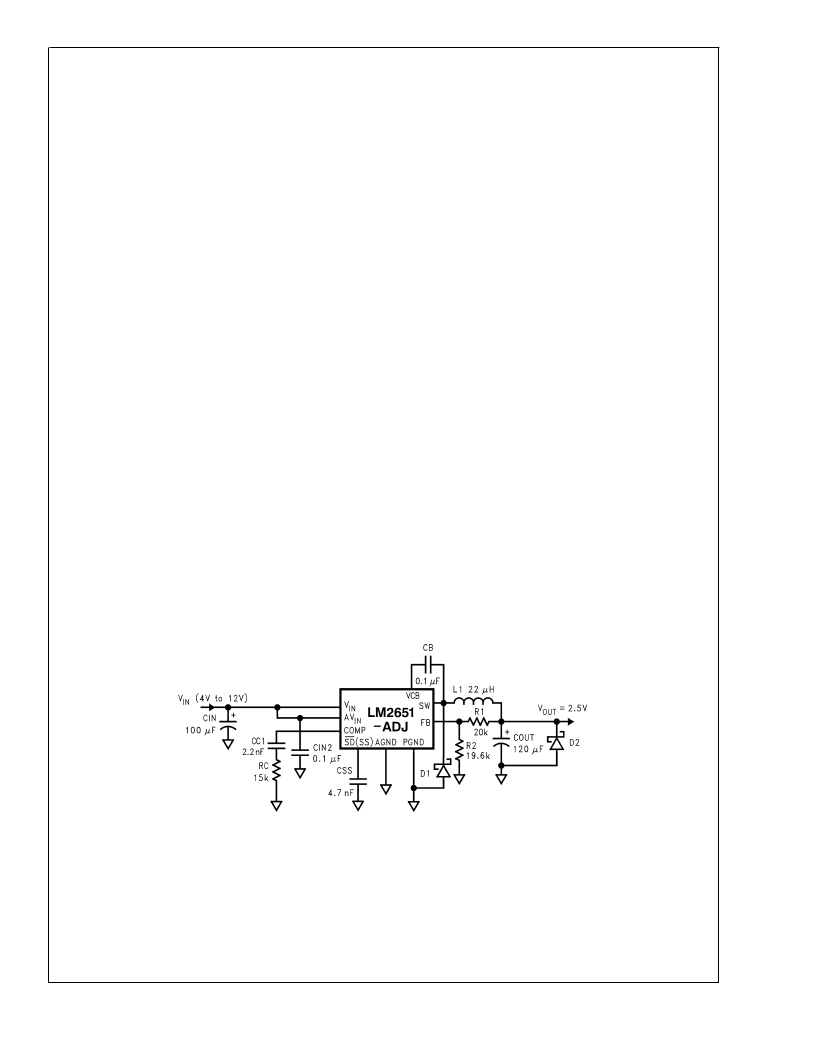
DS100925-23
Schematic for the Typical Board Layout
L
www.national.com
9
相關PDF資料 |
PDF描述 |
|---|---|
| LM2724ALD | High Speed 3A Synchronous MOSFET Driver |
| LM2724ALDX | High Speed 3A Synchronous MOSFET Driver |
| LM2724A | High Speed 3A Synchronous MOSFET Driver |
| LM2724AM | High Speed 3A Synchronous MOSFET Driver |
| LM2724AMX | High Speed 3A Synchronous MOSFET Driver |
相關代理商/技術參數 |
參數描述 |
|---|---|
| LM2651MTC-ADJ | 功能描述:直流/直流開關轉換器 RoHS:否 制造商:STMicroelectronics 最大輸入電壓:4.5 V 開關頻率:1.5 MHz 輸出電壓:4.6 V 輸出電流:250 mA 輸出端數量:2 最大工作溫度:+ 85 C 安裝風格:SMD/SMT |
| LM2651MTC-ADJ | 制造商:Texas Instruments 功能描述:SWITCHING REG 1.5A ADJ SMD 2651 |
| LM2651MTC-ADJ/NOPB | 功能描述:直流/直流開關轉換器 1.5A HIGH EFFICIENCY SWITCHING REG RoHS:否 制造商:STMicroelectronics 最大輸入電壓:4.5 V 開關頻率:1.5 MHz 輸出電壓:4.6 V 輸出電流:250 mA 輸出端數量:2 最大工作溫度:+ 85 C 安裝風格:SMD/SMT |
| LM2651MTCX-1.8 | 制造商:NSC 制造商全稱:National Semiconductor 功能描述:1.5A High Efficiency Synchronous Switching Regulator |
| LM2651MTCX-1.8/J7001113 | 制造商:Texas Instruments 功能描述: |
發布緊急采購,3分鐘左右您將得到回復。