- 您現在的位置:買賣IC網 > PDF目錄361025 > LM2796TLX (NATIONAL SEMICONDUCTOR CORP) Dual-Display White LED Driver with 3/2x Switched Capacitor Boost PDF資料下載
參數資料
| 型號: | LM2796TLX |
| 廠商: | NATIONAL SEMICONDUCTOR CORP |
| 元件分類: | 顯示驅動器 |
| 英文描述: | Dual-Display White LED Driver with 3/2x Switched Capacitor Boost |
| 中文描述: | LED DISPLAY DRIVER, PBGA18 |
| 封裝: | 2.10 X 2.40 MM, 0.60 MM HEIGHT, THIN MICRO SMD, 18 PIN |
| 文件頁數: | 4/8頁 |
| 文件大小: | 172K |
| 代理商: | LM2796TLX |
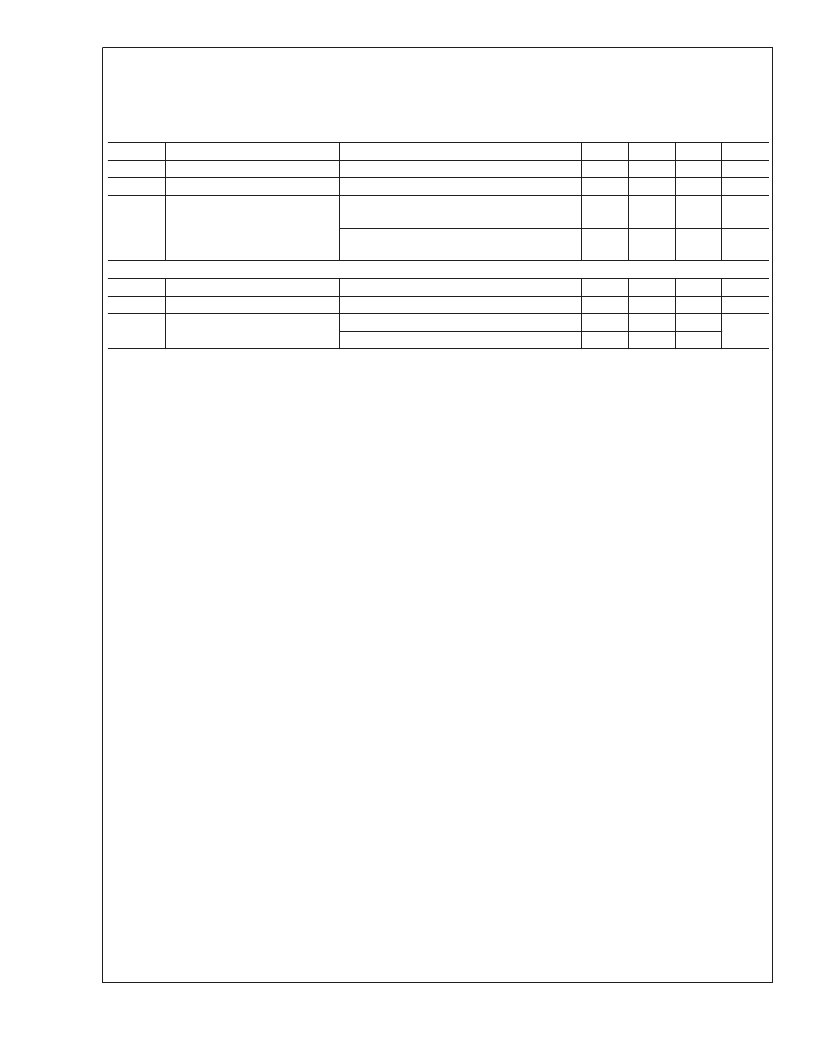
Electrical Characteristics
(Notes 2, 7) (Continued)
Limits in standard typeface and typical values apply for T
= 25
o
C. Limits in
boldface
type apply over the full operating junction
temperature range (-30C
≤
T
≤
+85C) . Unless otherwise specified: V
= 3.6V; V
= 3.6V; V(EN) = 2.0V; Group A and
Group B LEDs not ON simultaneously (ENA = V
IN
and ENB = GND, or ENA = GND and ENB = V
IN
); R
SET
= 8.35k
; C
IN
, C
1
,
C
2
, and C
POUT
= 1μF. (Note 8)
Symbol
Parameter
Condition
f
SW
Switching Frequency
3.0V
≤
V
IN
≤
4.2V
t
START
Start-up Time
I
Dx
= 90% steady state
1.5x/1x
Charge pump gain cross-over:
Gain = 1.5 when V
IN
is below
threshold. Gain = 1 when V
IN
is
above threshold.
Logic Pin Specifications: EN, ENA, ENB
V
IL
Input Logic Low
2.7V
≤
V
IN
≤
5.5V
V
IH
Input Logic High
2.7V
≤
V
IN
≤
5.5V
I
LEAK
Input Leakage Current
V
ENx
= 0V
V
ENx
= 3V (Note 13)
Min
325
Typ
500
100
4.75
Max
675
Units
kHz
μs
V
1.5x to 1x Threshold
1x to 1.5x Threshold
4.55
V
0
0.5
V
IN
V
V
μA
1.1
0.1
10
Note 1:
Absolute Maximum Ratings indicate limits beyond which damage to the component may occur. Operating Ratings are conditions under which operation of
the device is guaranteed. Operating Ratings do not imply guaranteed performance limits. For guaranteed performance limits and associated test conditions, see the
Electrical Characteristics tables.
Note 2:
All voltages are with respect to the potential at the GND pin.
Note 3:
Internal thermal shutdown circuitry protects the device from permanent damage. Thermal shutdown engages at T
J
= 160C (typ.) and disengages at T
J
=
120C (typ.). The thermal shutdown function is guaranteed by design.
Note 4:
The Human body model is a 100pF capacitor discharged through a 1.5k resistor into each pin. The machine model is a 200pF capacitor discharged directly
into each pin. MIL-STD-883 3015.7
Note 5:
In applications where high power dissipation and/or poor package thermal resistance is present, the maximum ambient temperature may have to be
derated. Maximum ambient temperature (T
A-MAX
) is dependent on the maximum operating junction temperature (T
J-MAX-OP
= 125C), the maximum power
dissipation of the device in the application (P
D-MAX
), and the junction-to ambient thermal resistance of the part/package in the application (
θ
JA
), as given by the
following equation: T
A-MAX
= T
J-MAX-OP
– (
θ
JA
x P
D-MAX
).
Note 6:
Junction-to-ambient thermal resistance is highly dependent on application and board layout. In applications where high maximum power dissipation exists,
special care must be paid to thermal dissipation issues in board design.
Note 7:
Min and Max limits are guaranteed by design, test, or statistical analysis. Typical numbers are not guaranteed, but do represent the most likely norm.
Note 8:
C
IN
, C
OUT
, C
1
, and C
2
: Low-ESR Surface-Mount Ceramic Capacitors (MLCCs) used in setting electrical characteristics
Note 9:
If both LED groups are to be ON simultaneously, the maximum V
Dxx
voltage may need to be derated, depending on minimum input voltage conditions. Refer
to the "MAXIMUM OUTPUT CURRENT, MAXIMUM LED VOLTAGE, MINIMUM INPUT VOLTAGE" section.
Note 10:
For the two groups of outputs on a part (Group A and Group B), the following are determined: the maximum output current in the group (MAX), the
minimum output current in the group (MIN), and the average output current of the group (AVG). For each group, two matching numbers are calculated:
(MAX-AVG)/AVG and (AVG-MIN)/AVG. The largest number of the two (worst case) is considered the matching figure for the group. The matching figure for a given
part is considered to be the highest matching figure of the two groups. The typical specification provided is the most likely norm of the matching figure for all parts.
Note 11:
Output resistance (R
OUT
) models all voltage losses in the charge pump. R
OUT
can be used to estimate the voltage at the charge pump output (P
OUT
):
V
Pout
= (1.5 x V
IN
) – (R
OUT
x I
OUT
). In the equation, I
OUT
is the total output current: the sum of all active Dxx output currents and all current drawn from P
OUT
. The
equation applies when the charge pump is operating with a gain of 3/2 (V
IN
≤
4.75V typ.).
Note 12:
Headroom voltage: V
HR
= V
Pout
– V
Dxx
. If headroom voltage requirement is not met, LED current regulation will be compromised.
Note 13:
There is a 300k
(typ.) pull-down resistor connected internally between each enable pin (EN, ENA, ENB) and GND.
L
www.national.com
4
相關PDF資料 |
PDF描述 |
|---|---|
| LM2796 | Dual-Display White LED Driver with 3/2x Switched Capacitor Boost |
| LM2925 | Cap-Free, NMOS, 150mA Low Dropout Regulator with Reverse Current Protection |
| LM2925T | Cap-Free, NMOS, 150mA Low Dropout Regulator with Reverse Current Protection |
| LM2926T | Cap-Free, NMOS, 150mA Low Dropout Regulator with Reverse Current Protection |
| LM2826 | Cap-Free, NMOS, 150mA Low Dropout Regulator with Reverse Current Protection |
相關代理商/技術參數 |
參數描述 |
|---|---|
| LM2796TLX/NOPB | 功能描述:LED照明驅動器 RoHS:否 制造商:STMicroelectronics 輸入電壓:11.5 V to 23 V 工作頻率: 最大電源電流:1.7 mA 輸出電流: 最大工作溫度: 安裝風格:SMD/SMT 封裝 / 箱體:SO-16N |
| LM2797 | 制造商:NSC 制造商全稱:National Semiconductor 功能描述:120mA High Efficiency Step-Down Switched Capacitor Voltage Converter with Voltage Monitoring |
| LM2797MM-1.8 | 制造商:Texas Instruments 功能描述:CONVERTER 120MA BUCK SMD MSOP10 |
| LM2797MM-1.8/NOPB | 功能描述:IC REG BUCK SWITCHED CAP 10-MSOP RoHS:是 類別:集成電路 (IC) >> PMIC - 穩壓器 - DC DC 開關穩壓器 系列:- 產品培訓模塊:Lead (SnPb) Finish for COTS Obsolescence Mitigation Program 標準包裝:1 系列:- 類型:降壓(降壓) 輸出類型:固定 輸出數:1 輸出電壓:3.3V 輸入電壓:4.5 V ~ 24 V PWM 型:- 頻率 - 開關:- 電流 - 輸出:125mA 同步整流器:無 工作溫度:-40°C ~ 85°C 安裝類型:表面貼裝 封裝/外殼:SOT-23-6 包裝:Digi-Reel® 供應商設備封裝:SOT-6 其它名稱:MAX1836EUT33#TG16DKR |
| LM2797MMX-1.8 | 功能描述:IC REG BUCK SWITCHED CAP 10MSOP RoHS:是 類別:集成電路 (IC) >> PMIC - 穩壓器 - DC DC 開關穩壓器 系列:- 產品培訓模塊:Lead (SnPb) Finish for COTS Obsolescence Mitigation Program 標準包裝:1 系列:- 類型:降壓(降壓) 輸出類型:固定 輸出數:1 輸出電壓:3.3V 輸入電壓:4.5 V ~ 24 V PWM 型:- 頻率 - 開關:- 電流 - 輸出:125mA 同步整流器:無 工作溫度:-40°C ~ 85°C 安裝類型:表面貼裝 封裝/外殼:SOT-23-6 包裝:Digi-Reel® 供應商設備封裝:SOT-6 其它名稱:MAX1836EUT33#TG16DKR |
發布緊急采購,3分鐘左右您將得到回復。