- 您現(xiàn)在的位置:買賣IC網(wǎng) > PDF目錄361025 > LM3075MTC (NATIONAL SEMICONDUCTOR CORP) High Efficiency, Synchronous Current Mode Buck Controller PDF資料下載
參數(shù)資料
| 型號(hào): | LM3075MTC |
| 廠商: | NATIONAL SEMICONDUCTOR CORP |
| 元件分類: | 穩(wěn)壓器 |
| 英文描述: | High Efficiency, Synchronous Current Mode Buck Controller |
| 中文描述: | SWITCHING CONTROLLER, 330 kHz SWITCHING FREQ-MAX, PDSO20 |
| 封裝: | TSSOP-20 |
| 文件頁(yè)數(shù): | 14/18頁(yè) |
| 文件大小: | 857K |
| 代理商: | LM3075MTC |
第1頁(yè)第2頁(yè)第3頁(yè)第4頁(yè)第5頁(yè)第6頁(yè)第7頁(yè)第8頁(yè)第9頁(yè)第10頁(yè)第11頁(yè)第12頁(yè)第13頁(yè)當(dāng)前第14頁(yè)第15頁(yè)第16頁(yè)第17頁(yè)第18頁(yè)
Output Capacitor Selection
(Continued)
input voltage is the highest and when the present switching
cycle has just finished. The corresponding minimum capaci-
tance is calculated as follows:
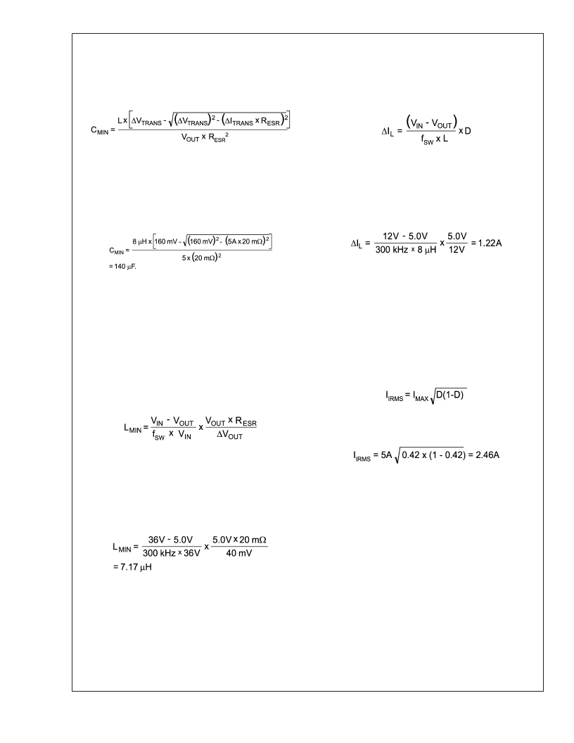
(8)
Notice it is already assumed the total ESR, R
esr
, is no
greater than R
esr_max
, otherwise the term under the square
root will be a negative value. Also, it is assumed that L has
already been selected, therefore the minimum L value
should be calculated before C
MIN
and after R
esr
(see Induc-
tor Selection below). Example: R
esr
= 20m
, V
OUT
= 5V,
V
TRANS
= 160mV,
I
TRANS
= 3A, L = 8μH
(9)
Generally speaking, C
decreases with decreasing R
,
I
, and L, but with increasing V
and
V
. The
output capacitance can therefore be chosen to be slightly
larger than the calculated value so that it is more easily
available. Here we would likely be fine choosing 220 μF.
Inductor Selection
The size of the output inductor can be determined from the
desired output ripple voltage,
V
OUT
, and the impedance of
the output capacitors at the switching frequency. The equa-
tion to determine the minimum inductance value is as fol-
lows:
(10)
In the above equation, R
is used in place of the imped-
ance of the output capacitors. This is because in most cases,
the impedance of the output capacitors at the switching
frequency is very close to R
. In the case of ceramic
capacitors, replace R
esr
with the true impedance.
Example:
V
IN_MAX
= 36V, V
OUT
= 5.0V,
V
OUT
= 40 mV, R
esr
= 20 m
, f
SW
(11)
The actual selection process usually involves several itera-
tions of all of the above steps, from ripple voltage selection,
to capacitor selection, to inductance calculations. Both the
highest and the lowest input and output voltages and load
transient requirements should be considered. If an induc-
tance value larger than L
MIN
is selected, make sure that the
C
MIN
requirement is not violated.
Priority should be given to parameters that are not flexible or
more costly. For example, if there are very few types of
capacitors to choose from, it may be a good idea to adjust
the inductance value so that a requirement of 3.2 capacitors
can be reduced to 3 capacitors.
Since inductor ripple current is often the criterion for select-
ing an output inductor, it is a good idea to double-check this
value. The equation is:
(12)
Where D is the duty cycle, defined by V
OUT
/V
IN
.
Also important is the ripple current, which is defined by
I
L
/I
NOM
., where I
NOM
is the nominal output current. Generally
speaking, a ripple content of less than 50% is ok. Larger
ripple content causes excessive losses in the inductor.
Example:
V
IN
= 12V, V
OUT
= 5.0V, f
SW
= 300 kHz, L = 8 μH
(13)
Given a maximum load current of 5A, the ripple content is
1.2A / 5A = 24%. When choosing an inductor, the saturation
current should be higher than the maximum peak inductor
current and the RMS current rating should be higher than the
maximum load current.
Input Capacitor Selection
The input capacitor must be selected such that it can handle
both the maximum ripple RMS current at highest ambient
temperature and the maximum input voltage. The equation
for the RMS current through the input capacitor is then
(14)
Where I
MAX
is maximum load current and D is the duty cycle.
Example: I
MAX
= 5A and D = 0.42
(15)
The function D(1-D) has a maxima at D = 0.5. This duty cycle
corresponds to the maximum RMS input current that may be
used as a worst case in selecting an input capacitor. Input
capacitors must meet the minimum requirements of voltage
and ripple current capacity. The size of the capacitor should
then be selected based on hold up time requirements. Bench
testing for individual applications is still the best way to
determine a reliable input capacitor value. The input capaci-
tor should always be placed as close as possible to the
current sense resistor or the drain of the top FET.
MOSFET Selection
BOTTOM FET SELECTION
During normal operation, the bottom FET is switching at
almost zero voltage and therefore only conduction losses
are present in the bottom FET. This makes the on resistance
(R
) the most important parameter when selecting the
bottom FET; the lower the on resistance, the lower the power
loss. The bottom FETs’ power losses peak at the maximum
L
www.national.com
14
相關(guān)PDF資料 |
PDF描述 |
|---|---|
| LM3075MTCX | High Efficiency, Synchronous Current Mode Buck Controller |
| LM3080 | Operational Transconductance Amplifier |
| LM3080AN | Operational Transconductance Amplifier |
| LM3080M | CAP 16V 470UF SOLID ELECT AXIAL |
| LM3080N | Operational Transconductance Amplifier |
相關(guān)代理商/技術(shù)參數(shù) |
參數(shù)描述 |
|---|---|
| LM3075MTC/NOPB | 功能描述:IC REG CTRLR BUCK PWM CM 20TSSOP RoHS:是 類別:集成電路 (IC) >> PMIC - 穩(wěn)壓器 - DC DC 切換控制器 系列:- 標(biāo)準(zhǔn)包裝:4,000 系列:- PWM 型:電壓模式 輸出數(shù):1 頻率 - 最大:1.5MHz 占空比:66.7% 電源電壓:4.75 V ~ 5.25 V 降壓:是 升壓:無(wú) 回掃:無(wú) 反相:無(wú) 倍增器:無(wú) 除法器:無(wú) Cuk:無(wú) 隔離:無(wú) 工作溫度:-40°C ~ 85°C 封裝/外殼:40-VFQFN 裸露焊盤 包裝:帶卷 (TR) |
| LM3075MTCX | 制造商:NSC 制造商全稱:National Semiconductor 功能描述:High Efficiency, Synchronous Current Mode Buck Controller |
| LM3075N/A+ | 制造商:未知廠家 制造商全稱:未知廠家 功能描述:FM Receiver Circuit |
| LM3075N/B+ | 制造商:未知廠家 制造商全稱:未知廠家 功能描述:FM Receiver Circuit |
| LM3075N-01/A+ | 制造商:未知廠家 制造商全稱:未知廠家 功能描述:FM Receiver Circuit |
發(fā)布緊急采購(gòu),3分鐘左右您將得到回復(fù)。