- 您現在的位置:買賣IC網 > PDF目錄361026 > LM3203TL (NATIONAL SEMICONDUCTOR CORP) Step-Down DC-DC Converter with Bypass Mode for CDMA / WCDMA RF Power Amplifiers PDF資料下載
參數資料
| 型號: | LM3203TL |
| 廠商: | NATIONAL SEMICONDUCTOR CORP |
| 元件分類: | 穩壓器 |
| 英文描述: | Step-Down DC-DC Converter with Bypass Mode for CDMA / WCDMA RF Power Amplifiers |
| 中文描述: | SWITCHING REGULATOR, 2200 kHz SWITCHING FREQ-MAX, BGA10 |
| 封裝: | LEAD FREE, THIN MICRO BUMP, 10 PIN |
| 文件頁數: | 4/15頁 |
| 文件大小: | 1360K |
| 代理商: | LM3203TL |
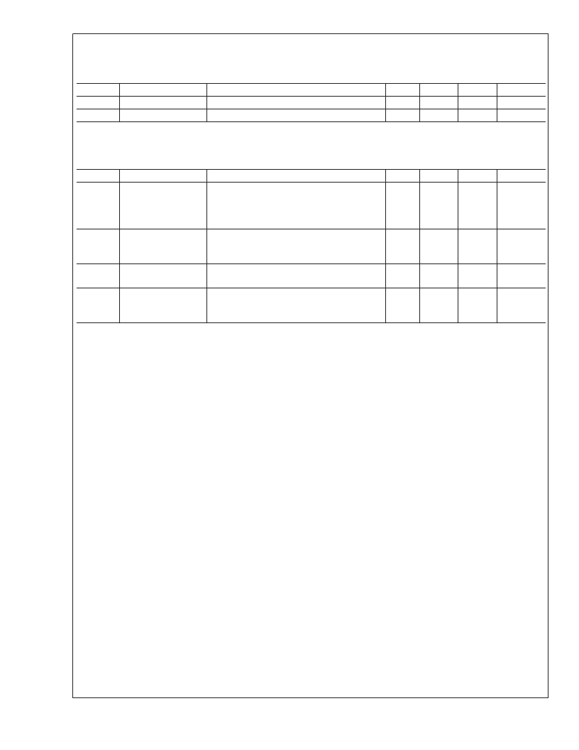
Electrical Characteristics
(Notes 2, 7) Limits in standard typeface are for T
A
= T
J
= 25C. Limits in
boldface
type apply over the full operating ambient temperature range (30C
≤
T
= T
≤
+85C). Unless otherwise noted,
specifications apply to the LM3203 with: PV
IN
= V
DD
= EN = 3.6V, BYP = 0V, V
CON
= 0.267V. (Continued)
Symbol
Gain
Z
CON
Parameter
Conditions
Min
Typ
1
1
Max
Units
V/V
M
V
CON
to V
OUT
Gain
V
CON
Input Resistance V
CON
= 1.2V
System Characteristics
range if the component values in the typical application circuit are used.
These parameters are not guaranteed by produc-
tion testing.
The following spec table entries are guaranteed by design over ambient temperature
Symbol
T
STARTUP
Time for V
OUT
to rise
to 3.4V in PWM mode
Parameter
Conditions
Min
Typ
50
Max
Units
μs
V
IN
= 4.2V, C
OUT
= 4.7μF,
R
LOAD
= 10
L = 3.3uH (I
SAT
>
0.94A)
EN = Low to High
V
IN
= 4.2V, C
OUT
= 4.7μF,
R
LOAD
= 10
L = 3.3uH (I
SAT
>
0.94A)
V
CON
= 1V,
Test frequency = 100kHz
V
IN
= 3.6V, V
CON
= 0.267V,
C
OUT
= 4.7μF, R
LOAD
= 10
BYP = Low to High
T
RESPONSE
Time for V
OUT
to Rise
from 0.8V to 3.6V in
PWM Mode
C
CON
V
CON
Input
Capacitance
T
ON_BYP
Bypass FET Turn On
Time In Bypass Mode
30
μs
15
pF
30
μs
Note 1:
Absolute Maximum Ratings indicate limits beyond which damage to the component may occur. Operating Ratings are conditions under which operation of
the device is guaranteed. Operating Ratings do not imply guaranteed performance limits. For guaranteed performance limits and associated test conditions, see the
Electrical Characteristics tables.
Note 2:
All voltages are with respect to the potential at the GND pins.
Note 3:
Internal thermal shutdown circuitry protects the device from permanent damage. Thermal shutdown engages at T
J
= 150C (typ.) and disengages at T
J
=
130C (typ.).
Note 4:
The Human body model is a 100pF capacitor discharged through a 1.5k
resistor into each pin. (MIL-STD-883 3015.7) . National Semiconductor
recommends that all integrated circuits be handled with appropriate precautions.
Note 5:
In applications where high power dissipation and/or poor package thermal resistance is present, the maximum ambient temperature may have to be
de-rated. Maximum ambient temperature (T
A-MAX
) is dependent on the maximum operating junction temperature (T
J-MAX-OP
= 125C), the maximum power
dissipation of the device in the application (P
D-MAX
), and the junction-to ambient thermal resistance of the part/package in the application (
θ
JA
), as given by the
following equation: T
A-MAX
= T
J-MAX-OP
– (
θ
JA
x P
D-MAX
).
Note 6:
Junction-to-ambient thermal resistance (
θ
JA
) is taken from thermal measurements, performed under the conditions and guidelines set forth in the JEDEC
standard JESD51-2. A 1" x 1", 4 layer, 1.5oz. Cu board was used for the measurements.
Note 7:
Min and Max limits are guaranteed by design, test, or statistical analysis. Typical numbers are not guaranteed, but do represent the most likely norm.
Note 8:
The LM3203 is designed for mobile phone applications where turn-on after power-up is controlled by the system controller and where requirements for a
small package size overrule increased die size for internal Under Voltage Lock-Out (UVLO) circuitry. Thus, it should be kept in shutdown by holding the EN pin low
until the input voltage exceeds 2.7V.
Note 9:
Over-Voltage protection (OVP) threshold is the voltage above the nominal V
OUT
where the OVP comparator turns off the PFET switch while in PWM mode.
The OVP threshold will be the value of the threshold at the FB voltage times the resistor divider ratio. In the
Figure 1
, 100mV (typ.) x ((267K + 133K) ÷ 133K).
Note 10:
Shutdown current includes leakage current of PFET and Bypass FET.
Note 11:
Electrical Characteristic table reflects open loop data (FB=0V and current drawn from SW pin ramped up until cycle by cycle current limit is activated).
Refer to datasheet curves for closed loop data and its variation with regards to supply voltage and temperature. Closed loop current limit is the peak inductor current
measured in the application circuit by increasing output current until output voltage drops by 10%.
Note 12:
Bypass FET current limit is defined as the load current at which the FB voltage is 1V lower than V
IN
.
L
www.national.com
4
相關PDF資料 |
PDF描述 |
|---|---|
| LM3203TLX | Step-Down DC-DC Converter with Bypass Mode for CDMA / WCDMA RF Power Amplifiers |
| LM326H | VOLTAGE REGULATORS |
| LM326N | VOLTAGE REGULATORS |
| LM326 | VOLTAGE REGULATORS |
| LM125 | VOLTAGE REGULATORS |
相關代理商/技術參數 |
參數描述 |
|---|---|
| LM3203TL/NOPB | 功能描述:DC/DC 開關控制器 RoHS:否 制造商:Texas Instruments 輸入電壓:6 V to 100 V 開關頻率: 輸出電壓:1.215 V to 80 V 輸出電流:3.5 A 輸出端數量:1 最大工作溫度:+ 125 C 安裝風格: 封裝 / 箱體:CPAK |
| LM3203TLEV | 功能描述:電源管理IC開發工具 LM3203 EVAL BOARD RoHS:否 制造商:Maxim Integrated 產品:Evaluation Kits 類型:Battery Management 工具用于評估:MAX17710GB 輸入電壓: 輸出電壓:1.8 V |
| LM3203TLX | 制造商:NSC 制造商全稱:National Semiconductor 功能描述:Step-Down DC-DC Converter with Bypass Mode for CDMA / WCDMA RF Power Amplifiers |
| LM3203TLX/J7002328 | 制造商:Rochester Electronics LLC 功能描述: 制造商:Texas Instruments 功能描述: |
| LM3203TLX/NOPB | 功能描述:DC/DC 開關控制器 RoHS:否 制造商:Texas Instruments 輸入電壓:6 V to 100 V 開關頻率: 輸出電壓:1.215 V to 80 V 輸出電流:3.5 A 輸出端數量:1 最大工作溫度:+ 125 C 安裝風格: 封裝 / 箱體:CPAK |
發布緊急采購,3分鐘左右您將得到回復。