- 您現在的位置:買賣IC網 > PDF目錄361028 > LM389N (NATIONAL SEMICONDUCTOR CORP) LM389 Low Voltage Audio Power Amplifier with NPN Transistor Array PDF資料下載
參數資料
| 型號: | LM389N |
| 廠商: | NATIONAL SEMICONDUCTOR CORP |
| 元件分類: | 音頻/視頻放大 |
| 英文描述: | LM389 Low Voltage Audio Power Amplifier with NPN Transistor Array |
| 中文描述: | 0.5 W, 1 CHANNEL, AUDIO AMPLIFIER, PDIP18 |
| 封裝: | 0.300 INCH, PLASTIC, DIP-18 |
| 文件頁數: | 2/8頁 |
| 文件大小: | 194K |
| 代理商: | LM389N |
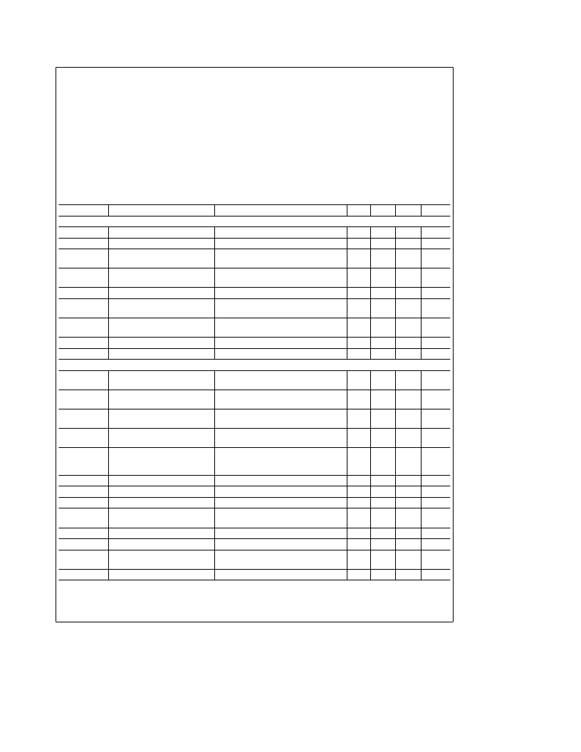
Absolute Maximum Ratings
If Military/Aerospace specified devices are required,
please contact the National Semiconductor Sales
Office/Distributors for availability and specifications.
Supply Voltage
Package Dissipation (Note 1)
Input Voltage
Storage Temperature
Operating Temperature
Junction Temperature
Lead Temperature (Soldering, 10 sec.)
Collector to Emitter Voltage, V
CEO
15V
1.89W
g
0.4V
b
65
§
C to
a
150
§
C
0
§
C to
a
70
§
C
150
§
C
260
§
C
12V
Collector to Base Voltage, V
CBO
Collector to Substrate Voltage, V
CIO
(Note 2)
Collector Current, I
C
Emitter Current, I
E
Base Current, I
B
Power Dissipation (Each Transistor) T
A
s
a
70
§
C
Thermal Resistance
i
JC
i
JA
15V
15V
25 mA
25 mA
5 mA
150 mW
24
§
C/W
70
§
C/W
Electrical Characteristics
T
A
e
25
§
C
Symbol
Parameter
Conditions
Min
Typ
Max
Units
AMPLIFIER
V
S
Operating Supply Voltage
4
12
V
I
Q
Quiescent Current
V
S
e
6V, V
IN
e
0V
6
12
mA
P
OUT
Output Power (Note 3)
THD
e
10%
V
S
e
6V, R
L
e
8
X
V
S
e
9V, R
L
e
16
X
250
325
500
mW
mW
A
V
Voltage Gain
V
S
e
6V, f
e
1 kHz
10
m
F from Pins 4 to 12
23
26
46
30
dB
dB
BW
Bandwidth
V
S
e
6V, Pins 4 and 12 Open
V
S
e
6V, R
L
e
8
X
, P
OUT
e
125 mW,
f
e
1 kHz, Pins 4 and 12 Open
V
S
e
6V, f
e
1 kHz, C
BYPASS
e
10
m
F,
Pins 4 and 12 Open, Referred to Output
250
kHz
THD
Total Harmonic Distortion
0.2
3.0
%
PSRR
Power Supply Rejection Ratio
30
50
dB
R
IN
Input Resistance
10
50
k
X
I
BIAS
Input Bias Current
V
S
e
6V, Pins 5 and 16 Open
250
nA
TRANSISTORS
V
CEO
Collector to Emitter
Breakdown Voltage
I
C
e
1 mA, I
B
e
0
12
20
V
V
CBO
Collector to Base
Breakdown Voltage
I
C
e
10
m
A, I
E
e
0
15
40
V
V
CIO
Collector to Substrate
Breakdown Voltage
I
C
e
10
m
A, I
E
e
I
B
e
0
15
40
V
V
EBO
Emitter to Base
Breakdown Voltage
I
E
e
10
m
A, I
C
e
0
6.4
7.1
7.8
V
H
FE
Static Forward Current
Transfer Ratio (Static Beta)
I
C
e
10
m
A
I
C
e
1 mA
I
C
e
10 mA
I
C
e
1 mA, V
CE
e
5V, f
e
1.0 kHz
I
E
e
1 mA
I
E
e
1 mA
I
C
e
10 mA, I
B
e
1 mA
100
275
275
100
h
oe
Open-Circuit Output Admittance
20
m
mho
V
BE
l
V
BE1
–V
BE2
l
V
CESAT
Base to Emitter Voltage
0.7
0.85
V
Base to Emitter Voltage Offset
1
5
mV
Collector to Emitter
Saturation Voltage
0.15
0.5
V
C
EB
Emitter to Base Capacitance
V
EB
e
3V
V
CB
e
3V
V
CI
e
3V
1.5
pF
C
CB
Collector to Base Capacitance
2
pF
C
CI
Collector to Substrate
Capacitance
3.5
pF
h
fe
Note 1:
For operation in ambient temperatures above 25
§
C, the device must be derated based on a 150
§
C maximum junction temperature and a thermal resistance
of 66
§
C/W junction to ambient.
Note 2:
The collector of each transistor is isolated from the substrate by an integral diode. Therefore, the collector voltage should remain positive with respect to
pin 17 at all times.
Note 3:
If oscillation exists under some load conditions, add 2.7
X
and 0.05
m
F series network from pin 1 to ground.
High Frequency Current Gain
I
C
e
10 mA, V
CE
e
5V, f
e
100 MHz
1.5
5.5
2
相關PDF資料 |
PDF描述 |
|---|---|
| LM389 | LM389 Low Voltage Audio Power Amplifier with NPN Transistor Array |
| LM3900M | LM2900/LM3900/LM3301 Quad Amplifiers |
| LM3900N | LM2900/LM3900/LM3301 Quad Amplifiers |
| LM3301 | LM2900/LM3900/LM3301 Quad Amplifiers |
| LM3301N | LM2900/LM3900/LM3301 Quad Amplifiers |
相關代理商/技術參數 |
參數描述 |
|---|---|
| LM389N/B+ | 制造商:未知廠家 制造商全稱:未知廠家 功能描述:Single Audio Amplifier |
| LM38W | 制造商:BEAVERSWOOD 功能描述:MARKER MAG WHITE 30X80MM PK100 |
| LM390 | 制造商:NSC 制造商全稱:National Semiconductor 功能描述:LM390 1W Battery Operated Audio Power Amplifier |
| LM3900 | 制造商:MOTOROLA 制造商全稱:Motorola, Inc 功能描述:QUAD SINGLE SUPPLY OPERATIONAL AMPLIFIERS |
| LM3900D | 功能描述:運算放大器 - 運放 Quad RoHS:否 制造商:STMicroelectronics 通道數量:4 共模抑制比(最小值):63 dB 輸入補償電壓:1 mV 輸入偏流(最大值):10 pA 工作電源電壓:2.7 V to 5.5 V 安裝風格:SMD/SMT 封裝 / 箱體:QFN-16 轉換速度:0.89 V/us 關閉:No 輸出電流:55 mA 最大工作溫度:+ 125 C 封裝:Reel |
發布緊急采購,3分鐘左右您將得到回復。