- 您現(xiàn)在的位置:買賣IC網(wǎng) > PDF目錄361028 > LM390 (National Semiconductor Corporation) LM390 1W Battery Operated Audio Power Amplifier PDF資料下載
參數(shù)資料
| 型號(hào): | LM390 |
| 廠商: | National Semiconductor Corporation |
| 英文描述: | LM390 1W Battery Operated Audio Power Amplifier |
| 中文描述: | LM390 1W的電動(dòng)音頻功率放大器 |
| 文件頁數(shù): | 3/6頁 |
| 文件大小: | 162K |
| 代理商: | LM390 |
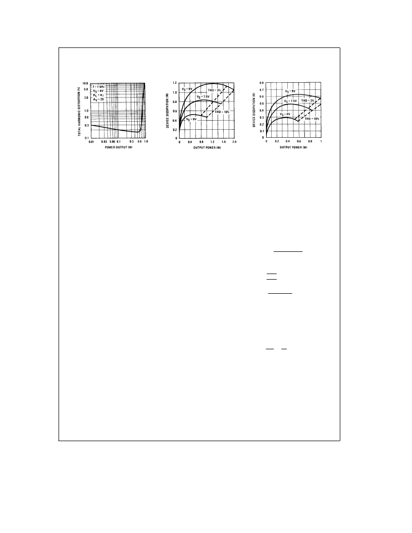
Typical Performance Characteristics
(Continued)
Distortion vs Output Power
Output Power 4
X
Load
Device Dissipation vs
Output Power 8
X
Load
Device Dissipation vs
TL/H/7848–6
Application Hints
Gain Control
To make the LM390 a more versatile amplifier, two pins (2
and 6) are provided for gain control. With pins 2 and 6 open,
the 1.35 k
X
resistor sets the gain at 20 (26 dB). If a capaci-
tor is put from pin 2 to 6, bypassing the 1.35 k
X
resistor, the
gain will go up to 200 (46 dB). If a resistor is placed in series
with the capacitor, the gain can be set to any value from 20
to 200. A low frequency pole in the gain response is caused
by the capacitor working against the external resistor in se-
ries with the 150
X
internal resistor. If the capacitor is elimi-
nated and a resistor connects pin 2 to 6 then the output dc
level may shift due to the additional dc gain. Gain control
can also be done by capacitively coupling a resistor (or
FET) from pin 6 to ground, as in Figure 7.
Additional external components can be placed in parallel
with the internal feedback resistors to tailor the gain and
frequency response for individual applications. For example,
we can compensate poor speaker bass response by fre-
quency shaping the feedback path. This is done with a se-
ries RC from pin 6 to 13 (paralleling the internal 15 k
X
resis-
tor). For 6 dB effective bass boost: R
j
15 k
X
, the lowest
value for good stable operation is R
e
10 k
X
if pin 2 is
open. If pins 2 and 6 are bypassed then R as low as 2 k
X
can be used. This restriction is because the amplifier is only
compensated for closed-loop gains greater than 9 V/V.
Input Biasing
The schematic shows that both inputs are biased to ground
with a 50 k
X
resistor. The base current of the input transis-
tors is about 250 nA, so the inputs are at about 12.5 mV
when left open. If the dc source resistance driving the
LM390 is higher than 250 k
X
it will contribute very little
additional offset (about 2.5 mV at the input, 50 mV at the
output). If the dc source resistance is less than 10 k
X
, then
shorting the unused input to ground will keep the offset low
(about 2.5 mV at the input 50 mV at the output). For dc
source resistances between these values we can eliminate
excess offset by putting a resistor from the unused input to
ground, equal in value to the dc source resistance. Of
course all offset problems are eliminated if the input is ca-
pacitively coupled.
When using the LM390 with higher gains (bypassing the
1.35 k
X
resistor between pins 2 and 6) it is necessary to
bypass the unused input, preventing degradation of gain
and possible instabilities. This is done with a 0.1
m
F capaci-
tor or a short to ground depending on the dc source resist-
ance on the driven input.
Bootstrapping
The base of the output transistor of the LM390 is brought
out to pin 9 for Bootstrapping. The output stage of the am-
plifier during positive swing is shown in Figure 3 with its
external circuitry.
R1
a
R2 set the amount of base current available to the
output transistor. The maximum output current divided by
beta is the value required for the current in R1 and R2:
(R1
a
R2)
e
b
O
I
O MAX
e
0
(V
S
/2)
b
V
BE
I
O MAX
0.632
Good design values are V
BE
e
0.7V and
b
O
e
100.
Example 0.8 watt into 4
X
load with V
S
e
6V.
2 P
O
R
L
(6/2)
b
0.7
e
632 mA
(R1
a
R2)
e
100
#
e
364
X
To keep the current in R2 constant during positive swing
capacitor C
B
is added. As the output swings positive C
B
lifts
R1 and R2 above the supply, maintaining a constant voltage
across R2. To minimize the value of C
B
, R1
e
R2. The pole
due to C
B
and R1 and R2 is usually set equal to the pole
due to the output coupling capacitor and the load. This
gives:
C
B
j
4C
c
b
O
j
C
c
25
Example: for 100 Hz pole and R
L
e
4
X
; C
c
e
400
m
F and
C
B
e
16
m
F, if R1 is made a diode and R2 increased to give
the same current, C
B
can be decreased by about a factor of
4, as in Figure 4.
For reduced component count the load can replace R1. The
value of (R1
a
R2) is the same, so R2 is increased. Now C
B
is both the coupling and the bootstrapping capacitor (see
Figure 2).
3
相關(guān)PDF資料 |
PDF描述 |
|---|---|
| LM390N | LM390 1W Battery Operated Audio Power Amplifier |
| LM3911 | LM3911 Temperature Controller |
| LM3911H-46 | LM3911 Temperature Controller |
| LM3911N | LM3911 Temperature Controller |
| LM3914 | Dot/Bar Display Driver |
相關(guān)代理商/技術(shù)參數(shù) |
參數(shù)描述 |
|---|---|
| LM3900 | 制造商:MOTOROLA 制造商全稱:Motorola, Inc 功能描述:QUAD SINGLE SUPPLY OPERATIONAL AMPLIFIERS |
| LM3900D | 功能描述:運(yùn)算放大器 - 運(yùn)放 Quad RoHS:否 制造商:STMicroelectronics 通道數(shù)量:4 共模抑制比(最小值):63 dB 輸入補(bǔ)償電壓:1 mV 輸入偏流(最大值):10 pA 工作電源電壓:2.7 V to 5.5 V 安裝風(fēng)格:SMD/SMT 封裝 / 箱體:QFN-16 轉(zhuǎn)換速度:0.89 V/us 關(guān)閉:No 輸出電流:55 mA 最大工作溫度:+ 125 C 封裝:Reel |
| LM3900DE4 | 功能描述:運(yùn)算放大器 - 運(yùn)放 Quadruple Oper Amplifier RoHS:否 制造商:STMicroelectronics 通道數(shù)量:4 共模抑制比(最小值):63 dB 輸入補(bǔ)償電壓:1 mV 輸入偏流(最大值):10 pA 工作電源電壓:2.7 V to 5.5 V 安裝風(fēng)格:SMD/SMT 封裝 / 箱體:QFN-16 轉(zhuǎn)換速度:0.89 V/us 關(guān)閉:No 輸出電流:55 mA 最大工作溫度:+ 125 C 封裝:Reel |
| LM3900DG4 | 功能描述:運(yùn)算放大器 - 運(yùn)放 Quad Op Amp RoHS:否 制造商:STMicroelectronics 通道數(shù)量:4 共模抑制比(最小值):63 dB 輸入補(bǔ)償電壓:1 mV 輸入偏流(最大值):10 pA 工作電源電壓:2.7 V to 5.5 V 安裝風(fēng)格:SMD/SMT 封裝 / 箱體:QFN-16 轉(zhuǎn)換速度:0.89 V/us 關(guān)閉:No 輸出電流:55 mA 最大工作溫度:+ 125 C 封裝:Reel |
| LM3900DR | 功能描述:運(yùn)算放大器 - 運(yùn)放 Quad Op Amp RoHS:否 制造商:STMicroelectronics 通道數(shù)量:4 共模抑制比(最小值):63 dB 輸入補(bǔ)償電壓:1 mV 輸入偏流(最大值):10 pA 工作電源電壓:2.7 V to 5.5 V 安裝風(fēng)格:SMD/SMT 封裝 / 箱體:QFN-16 轉(zhuǎn)換速度:0.89 V/us 關(guān)閉:No 輸出電流:55 mA 最大工作溫度:+ 125 C 封裝:Reel |
發(fā)布緊急采購,3分鐘左右您將得到回復(fù)。