- 您現(xiàn)在的位置:買賣IC網(wǎng) > PDF目錄361028 > LM3914 (National Semiconductor Corporation) Dot/Bar Display Driver PDF資料下載
參數(shù)資料
| 型號(hào): | LM3914 |
| 廠商: | National Semiconductor Corporation |
| 英文描述: | Dot/Bar Display Driver |
| 中文描述: | 點(diǎn)/酒吧顯示驅(qū)動(dòng)程序 |
| 文件頁(yè)數(shù): | 3/19頁(yè) |
| 文件大小: | 365K |
| 代理商: | LM3914 |
第1頁(yè)第2頁(yè)當(dāng)前第3頁(yè)第4頁(yè)第5頁(yè)第6頁(yè)第7頁(yè)第8頁(yè)第9頁(yè)第10頁(yè)第11頁(yè)第12頁(yè)第13頁(yè)第14頁(yè)第15頁(yè)第16頁(yè)第17頁(yè)第18頁(yè)第19頁(yè)
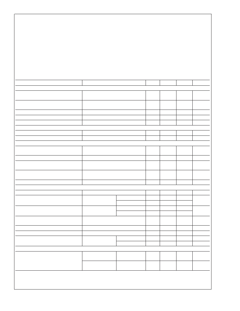
Absolute Maximum Ratings
(Note 1)
If Military/Aerospace specified devices are required,
please contact the National Semiconductor Sales Office/
Distributors for availability and specifications.
Power Dissipation (Note 6)
Molded DIP (N)
Supply Voltage
Voltage on Output Drivers
Input Signal Overvoltage (Note 4)
Divider Voltage
1365 mW
25V
25V
±
35V
100 mV to V
+
Reference Load Current
Storage Temperature Range
Soldering Information
Dual-In-Line Package
Soldering (10 seconds)
Plastic Chip Carrier Package
Vapor Phase (60 seconds)
Infrared (15 seconds)
See AN-450 “Surface Mounting Methods and Their Effect
on Product Reliability” for other methods of soldering
surface mount devices.
10 mA
55C to +150C
260C
215C
220C
Electrical Characteristics
(Notes 2, 4)
Parameter
Conditions
(Note 2)
Min
Typ
Max
Units
COMPARATOR
Offset Voltage, Buffer and First
Comparator
Offset Voltage, Buffer and Any Other
Comparator
Gain (
I
LED
/
V
IN
)
Input Bias Current (at Pin 5)
Input Signal Overvoltage
VOLTAGE-DIVIDER
Divider Resistance
Accuracy
VOLTAGE REFERENCE
Output Voltage
0V
≤
V
= V
RHI
≤
12V,
I
LED
= 1 mA
0V
≤
V
= V
RHI
≤
12V,
I
LED
= 1 mA
I
L(REF)
= 2 mA, I
LED
= 10 mA
0V
≤
V
IN
≤
V
+
1.5V
No Change in Display
3
10
mV
3
15
mV
3
8
mA/mV
nA
V
25
100
35
35
Total, Pin 6 to 4
(Note 3)
8
12
0.5
17
2
k
%
0.1 mA
≤
I
L(REF)
≤
4 mA,
V
+
= V
LED
= 5V
3V
≤
V
+
≤
18V
0.1 mA
≤
I
L(REF)
≤
4 mA,
V
+
= V
LED
0C
≤
T
A
≤
+70C, I
L(REF)
= 1 mA,
V
+
= 5V
1.2
1.28
1.34
V
Line Regulation
Load Regulation
0.01
0.03
%/V
0.4
2
%
Output Voltage Change with
Temperature
Adjust Pin Current
OUTPUT DRIVERS
LED Current
1
%
75
120
μA
V
+
= V
LED
= 5V, I
L(REF)
= 1 mA
V
LED
= 5V
7
10
0.12
1.2
0.1
1
13
0.4
3
0.25
3
mA
LED Current Difference (Between
Largest and Smallest LED Currents)
I
LED
= 2 mA
I
LED
= 20 mA
I
LED
= 2 mA
I
LED
= 20 mA
mA
LED Current Regulation
2V
≤
V
LED
≤
17V
mA
Dropout Voltage
I
LED(ON)
= 20 mA, V
LED
= 5V,
I
LED
= 2 mA
I
LED
= 2.0 mA, I
L(REF)
= 0.4 mA
(Bar Mode) (Note 5)
(Dot Mode)
(Note 5)
1.5
V
Saturation Voltage
Output Leakage, Each Collector
Output Leakage
0.15
0.1
0.1
150
0.4
10
10
450
V
μA
μA
μA
Pins 10–18
Pin 1
60
SUPPLY CURRENT
Standby Supply Current
(All Outputs Off)
V
+
= 5V,
I
L(REF)
= 0.2 mA
V
+
= 20V,
I
L(REF)
= 1.0 mA
2.4
4.2
mA
6.1
9.2
mA
Note 1:
Absolute Maximum Ratings indicate limits beyond which damage to the device may occur. Operating Ratings indicate conditions for which the device is func-
tional, but do not guarantee specific performance limits. Electrical Characteristics state DC andAC electrical specifications under particular test conditions which guar-
antee specific performance limits. This assumes that the device is within the Operating Ratings. Specifications are not guaranteed for parameters where no limit is
given, however, the typical value is a good indication of device performance.
L
www.national.com
3
相關(guān)PDF資料 |
PDF描述 |
|---|---|
| LM3914N | Dot/Bar Display Driver |
| LM3914V | Dot/Bar Display Driver |
| LM3914N-1 | MULTI DVI TRANSMITTER -FIBER |
| LM3916 | Dot/Bar Display Driver |
| LM3916N | Dot/Bar Display Driver |
相關(guān)代理商/技術(shù)參數(shù) |
參數(shù)描述 |
|---|---|
| LM3914_03 | 制造商:NSC 制造商全稱:National Semiconductor 功能描述:Dot/Bar Display Driver |
| LM3914J/A+ | 制造商:未知廠家 制造商全稱:未知廠家 功能描述:LED Display Driver |
| LM3914N | 制造商:Texas Instruments 功能描述:3914 NAT'90 SB175D 制造商:NAT'L SEMI 功能描述: 制造商:Texas Instruments 功能描述:IC BAR GRAPH DRIVER |
| LM3914N/A+ | 制造商:未知廠家 制造商全稱:未知廠家 功能描述:LED Display Driver |
| LM3914N/B+ | 制造商:未知廠家 制造商全稱:未知廠家 功能描述:LED Display Driver |
發(fā)布緊急采購(gòu),3分鐘左右您將得到回復(fù)。