- 您現在的位置:買賣IC網 > PDF目錄361028 > LM3914N-1 (NATIONAL SEMICONDUCTOR CORP) MULTI DVI TRANSMITTER -FIBER PDF資料下載
參數資料
| 型號: | LM3914N-1 |
| 廠商: | NATIONAL SEMICONDUCTOR CORP |
| 元件分類: | 顯示驅動器 |
| 英文描述: | MULTI DVI TRANSMITTER -FIBER |
| 中文描述: | LED DISPLAY DRIVER, PDIP18 |
| 封裝: | PLASTIC, DIP-18 |
| 文件頁數: | 4/19頁 |
| 文件大小: | 365K |
| 代理商: | LM3914N-1 |
Electrical Characteristics
(Notes 2, 4) (Continued)
Note 2:
Unless otherwise stated, all specifications apply with the following conditions:
3 V
DC
≤
V
+
≤
20 V
DC
3 V
DC
≤
V
LED
≤
V
+
0.015V
≤
V
RLO
≤
12 V
DC
T
A
= +25C, I
L(REF)
= 0.2 mA, V
LED
= 3.0V, pin 9 connected to pin 3 (Bar Mode).
0.015V
≤
V
RHI
≤
12 V
DC
For higher power dissipations, pulse testing is used.
Note 3:
Accuracy is measured referred to +10.000 V
DC
at pin 6, with 0.000 V
DC
at pin 4. At lower full-scale voltages, buffer and comparator offset voltage may add
significant error.
Note 4:
Pin 5 input current must be limited to
±
3 mA. The addition of a 39k resistor in series with pin 5 allows
±
100V signals without damage.
Note 5:
Bar mode results when pin 9 is within 20 mV of V
+
. Dot mode results when pin 9 is pulled at least 200 mV below V
+
or left open circuit. LED No. 10 (pin
10 output current) is disabled if pin 9 is pulled 0.9V or more below V
LED
.
Note 6:
The maximum junction temperature of the LM3914 is 100C. Devices must be derated for operation at elevated temperatures. Junction to ambient thermal
resistance is 55C/W for the molded DIP (N package).
V
REF
, V
RHI
, V
RLO
≤
(V
+
1.5V)
0V
≤
V
IN
≤
V
+
1.5V
Definition of Terms
Accuracy:
The difference between the observed threshold
voltage and the ideal threshold voltage for each comparator.
Specified and tested with 10V across the internal voltage di-
vider so that resistor ratio matching error predominates over
comparator offset voltage.
Adjust Pin Current:
Current flowing out of the reference ad-
just pin when the reference amplifier is in the linear region.
Comparator Gain:
The ratio of the change in output current
(I
) to the change in input voltage (V
) required to pro-
duce it for a comparator in the linear region.
Dropout Voltage:
The voltage measured at the current
source outputs required to make the output current fall by
10%.
Input Bias Current:
Current flowing out of the signal input
when the input buffer is in the linear region.
Typical Performance Characteristics
LED Current Regulation:
The change in output current
over the specified range of LED supply voltage (V
) as
measured at the current source outputs. As the forward volt-
age of an LED does not change significantly with a small
change in forward current, this is equivalent to changing the
voltage at the LED anodes by the same amount.
Line Regulation:
The average change in reference output
voltage over the specified range of supply voltage (V
+
).
Load Regulation:
The change in reference output voltage
(V
REF
) over the specified range of load current (I
L(REF)
).
Offset Voltage:
The differential input voltage which must be
applied to each comparator to bias the output in the linear re-
gion. Most significant error when the voltage across the in-
ternal voltage divider is small. Specified and tested with pin
6 voltage (V
RHI
) equal to pin 4 voltage (V
RLO
).
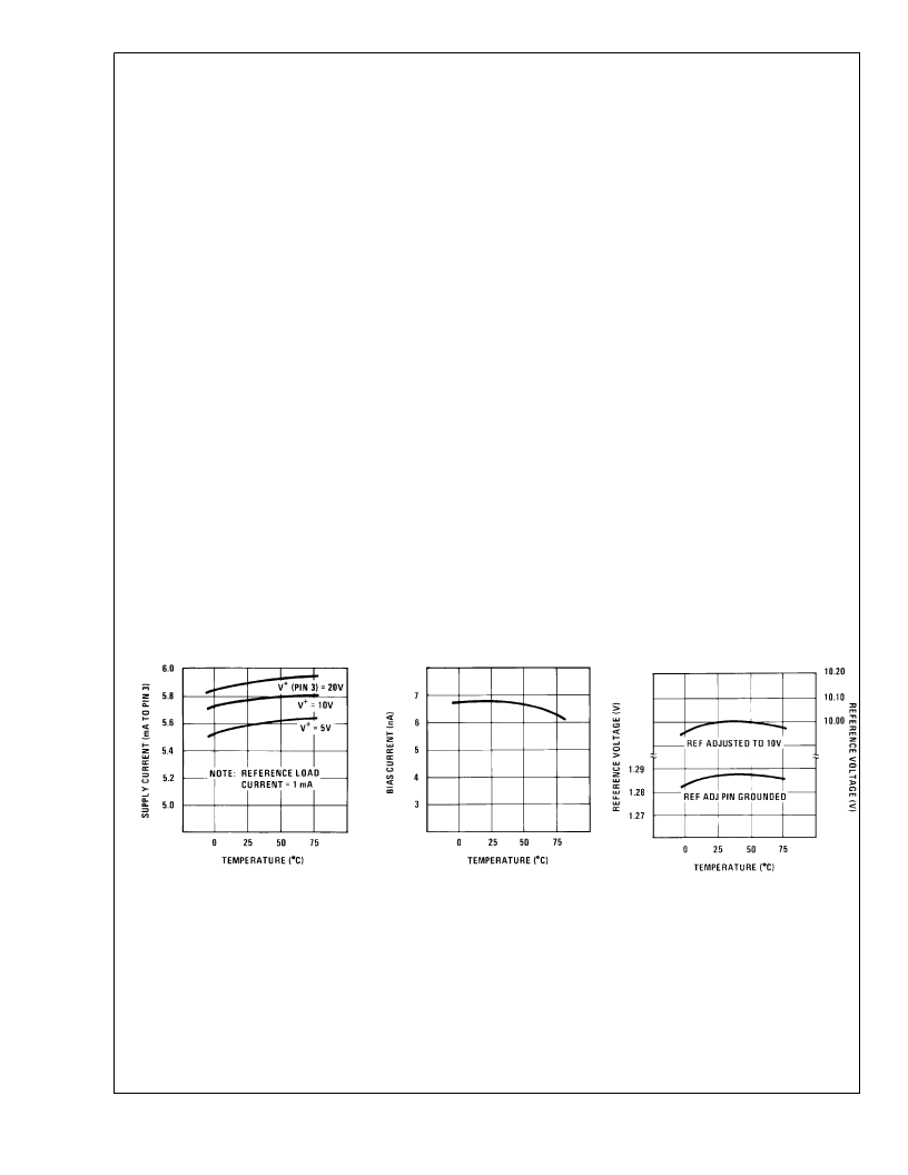
Supply Current vs
Temperature
DS007970-2
Operating Input Bias
Current vs Temperature
DS007970-20
Reference Voltage vs
Temperature
DS007970-21
L
www.national.com
4
相關PDF資料 |
PDF描述 |
|---|---|
| LM3916 | Dot/Bar Display Driver |
| LM3916N | Dot/Bar Display Driver |
| LM3916N-1 | 6 PIN MINI DIN CABLE MM 50FT |
| LM395 | Ultra Reliable Power Transistors |
| LM395T | Ultra Reliable Power Transistors |
相關代理商/技術參數 |
參數描述 |
|---|---|
| LM3914N-1 | 制造商:Texas Instruments 功能描述:LED BAR GRAPH DRIVER 3914 DIP18 |
| LM3914N-1/HALF | 制造商:Texas Instruments 功能描述:LED BAR GRAPH DRIVER 3914 DIP18 |
| LM3914N-1/NOPB | 功能描述:LED照明驅動器 DOT/BAR DISPLAY DRVR RoHS:否 制造商:STMicroelectronics 輸入電壓:11.5 V to 23 V 工作頻率: 最大電源電流:1.7 mA 輸出電流: 最大工作溫度: 安裝風格:SMD/SMT 封裝 / 箱體:SO-16N |
| LM3914N-1/NOPB | 制造商:Texas Instruments 功能描述:LED Driver IC |
| LM3914V | 功能描述:LED照明驅動器 RoHS:否 制造商:STMicroelectronics 輸入電壓:11.5 V to 23 V 工作頻率: 最大電源電流:1.7 mA 輸出電流: 最大工作溫度: 安裝風格:SMD/SMT 封裝 / 箱體:SO-16N |
發布緊急采購,3分鐘左右您將得到回復。