- 您現(xiàn)在的位置:買賣IC網(wǎng) > PDF目錄361029 > LM4892 (National Semiconductor Corporation) 1 Watt Audio Power Amplifier with Headphone Sense PDF資料下載
參數(shù)資料
| 型號: | LM4892 |
| 廠商: | National Semiconductor Corporation |
| 英文描述: | 1 Watt Audio Power Amplifier with Headphone Sense |
| 中文描述: | 1瓦音頻功率放大器意識與耳機(jī) |
| 文件頁數(shù): | 12/22頁 |
| 文件大小: | 1037K |
| 代理商: | LM4892 |
Application Information
(Continued)
create pops upon device enable. Thus, by minimizing the
capacitor size based on necessary low frequency response,
turn-on pops can be minimized.
Besides minimizing the input capacitor size, careful consid-
eration should be paid to the bypass capacitor value. Bypass
capacitor, C
, is the most critical component to minimize
turn-on pops since it determines how fast the LM4892 turns
on. The slower the LM4892’s outputs ramp to their quiescent
DC voltage (nominally 1/2 V
), the smaller the turn-on pop.
Choosing C
equal to 1.0μF along with a small value of C
(in
the range of 0.1μF to 0.39μF), should produce a virtually
clickless and popless shutdown function. While the device
will function properly, (no oscillations or motorboating), with
C
equal to 0.1μF, the device will be much more susceptible
to turn-on clicks and pops. Thus, a value of C
equal to
1.0μF is recommended in all but the most cost sensitive
designs.
AUDIO POWER AMPLIFIER DESIGN
A 1W/8
AUDIO AMPLIFIER
Given:
Power Output
Load Impedance
Input Level
Input Impedance
Bandwidth
1 Wrms
8
1 Vrms
20 k
100 Hz–20 kHz
±
0.25 dB
A designer must first determine the minimum supply rail to
obtain the specified output power. By extrapolating from the
Output Power vs Supply Voltage graphs in the
Typical Per-
formance Characteristics
section, the supply rail can be
easily found. A second way to determine the minimum sup-
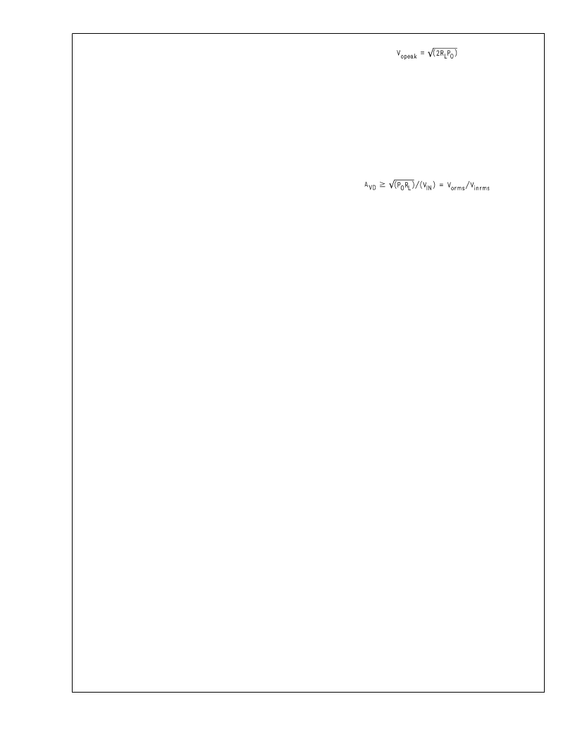
ply rail is to calculate the required V
opeak
using Equation 2
and add the output voltage. Using this method, the minimum
supply voltage would be (V
opeak
+ (V
OD
+ V
OD
)), where
V
OD
and V
OD
are extrapolated from the Dropout Volt-
age vs Supply Voltage curve in the
Typical Performance
Characteristics
section.
(2)
5V is a standard voltage in most applications, it is chosen for
the supply rail. Extra supply voltage creates headroom that
allows the LM4892 to reproduce peaks in excess of 1W
without producing audible distortion. At this time, the de-
signer must make sure that the power supply choice along
with the output impedance does not violate the conditions
explained in the
Power Dissipation
section.
Once the power dissipation equations have been addressed,
the required differential gain can be determined from Equa-
tion 3.
(3)
R
f
/R
i
= A
VD
/2
From Equation 3, the minimum A
VD
is 2.83; use A
VD
= 3.
Since the desired input impedance was 20k
, and with a
A
VD
of 3, a ratio of 1.5:1 of R
to R
results in an allocation of
R
= 20k
and R
= 30k
. The final design step is to address
the bandwidth requirements which must be stated as a pair
of 3dB frequency points. Five times away from a 3dB point
is 0.17dB down from passband response which is better
than the required
±
0.25dB specified.
f
L
= 100Hz/5 = 20Hz
f
H
= 20kHz * 5 = 100kHz
As stated in the
External Components
section, R
i
in con-
junction with C
i
create a highpass filter.
C
i
≥
1/(2
π
*20 k
*20 Hz) = 0.397 μF; use 0.39 μF
The high frequency pole is determined by the product of the
desired frequency pole, f
H
, and the differential gain, A
VD
.
With a A
VD
= 3 and f
H
= 100kHz, the resulting GBWP =
150kHz which is much smaller than the LM4892 GBWP of
4 MHz. This figure displays that if a designer has a need to
design an amplifier with a higher differential gain, the
LM4892 can still be used without running into bandwidth
limitations.
L
www.national.com
12
相關(guān)PDF資料 |
PDF描述 |
|---|---|
| LM4892IBP | 1 Watt Audio Power Amplifier with Headphone Sense |
| LM4892IBPX | 1 Watt Audio Power Amplifier with Headphone Sense |
| LM4894MM | 1 Watt Fully Differential Audio Power Amplifier With Shutdown Select |
| LM4894 | 1 Watt Fully Differential Audio Power Amplifier With Shutdown Select |
| LM4894IBP | 1 Watt Fully Differential Audio Power Amplifier With Shutdown Select |
相關(guān)代理商/技術(shù)參數(shù) |
參數(shù)描述 |
|---|---|
| LM48920B WAF | 制造商:Texas Instruments 功能描述: |
| LM4892B E WAF | 制造商:Texas Instruments 功能描述: |
| LM4892BUPN E WAF | 制造商:Texas Instruments 功能描述: |
| LM4892IBP | 功能描述:IC AMP AUDIO PWR 1W MONO 8USMD RoHS:否 類別:集成電路 (IC) >> 線性 - 音頻放大器 系列:Boomer® 產(chǎn)品培訓(xùn)模塊:Lead (SnPb) Finish for COTS Obsolescence Mitigation Program 標(biāo)準(zhǔn)包裝:2,500 系列:DirectDrive® 類型:H 類 輸出類型:耳機(jī),2-通道(立體聲) 在某負(fù)載時最大輸出功率 x 通道數(shù)量:35mW x 2 @ 16 歐姆 電源電壓:1.62 V ~ 1.98 V 特點(diǎn):I²C,麥克風(fēng),靜音,短路保護(hù),音量控制 安裝類型:表面貼裝 供應(yīng)商設(shè)備封裝:25-WLP(2.09x2.09) 封裝/外殼:25-WFBGA,WLCSP 包裝:帶卷 (TR) |
| LM4892IBPX | 制造商:Rochester Electronics LLC 功能描述:1W AUDIO AMP WITH HEADPHONE SE - Bulk |
發(fā)布緊急采購,3分鐘左右您將得到回復(fù)。