- 您現在的位置:買賣IC網 > PDF目錄361030 > LM5026MT (NATIONAL SEMICONDUCTOR CORP) Active Clamp Current Mode PWM Controller PDF資料下載
參數資料
| 型號: | LM5026MT |
| 廠商: | NATIONAL SEMICONDUCTOR CORP |
| 元件分類: | 穩壓器 |
| 英文描述: | Active Clamp Current Mode PWM Controller |
| 中文描述: | 3 A SWITCHING CONTROLLER, 660 kHz SWITCHING FREQ-MAX, PDSO16 |
| 封裝: | TSSOP-16 |
| 文件頁數: | 17/23頁 |
| 文件大小: | 936K |
| 代理商: | LM5026MT |
Applications Information
(Continued)
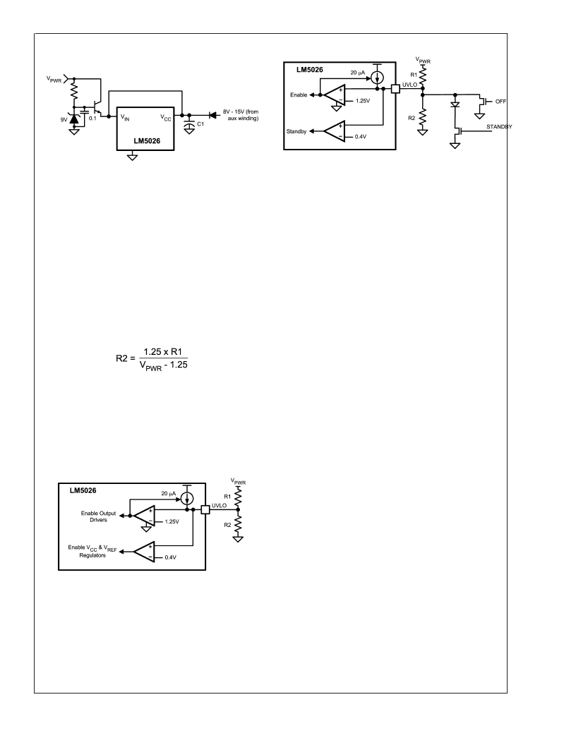
UNDER-VOLTAGE LOCKOUT (UVLO)
When the UVLO pin voltage is below 0.4V the controller is in
a low current shutdown mode. When the UVLO pin voltage is
greater than 0.4V but less than 1.25V the controller is in
standby mode. When the UVLO pin voltage is greater than
1.25V the controller is fully enabled. Typically, two external
resistors program the minimum operational voltage for the
power converter as shown in
Figure 13
. When UVLO pin
voltage is above the 1.25V threshold, an internal 20 μA
current source is enabled to raise the voltage at the UVLO
pin, thus providing threshold hysteresis. Resistance values
for R1 and R2 can be determined from:
R1 = V
HYS
/ 20 μA
Where V
is the desired turn-on voltage and V
is the
desired UVLO hysteresis at V
. For example, if the
LM5026 is to be enabled when V
reaches 33V, and
disabled when V
is decreased to 30V, R1 calculates to
150 k
, and R2 calculates to 5.9 k
. The voltage at the
UVLO pin should not exceed 6V at any time. Be sure to
check both the power and voltage rating for the selected R1
resistor.
Remote configuration of the controller’s operational modes
can be accomplished with open drain device(s) connected to
the UVLO pin as shown in
Figure 14
.
OSCILLATOR (RT, SYNC)
Oscillator (RT, SYNC) The oscillator frequency is generally
selected in conjunction with the design of the system mag-
netic components along with the volume and efficiency goals
for a given power converter design. The total RT resistance
at the RT pin sets the oscillator frequency. The RT resistors
should be one of the first components placed and connected
when designing the PC board. Direct, short connections to
each side of the RT resistors (RT, DCL and AGND pins) are
recommended .
The SYNC pin can be used to synchronize the internal
oscillator to an external clock. An open drain output is the
recommended interface from the external clock to the SYNC
pin. The clock pulse width should be greater than 15 ns. The
external clock must be a
higher frequency
than the free
running frequency set by the RT resistor. Multiple LM5026
devices can be synchronized together simply by connecting
the devices SYNC pins together. Care should be taken to
ensure the ground potential differences between devices are
minimized. In this configuration all of the devices will be
synchronized to the highest frequency device.
VOLTAGE FEEDBACK (COMP)
The COMP pin is designed to accept the voltage loop feed-
back error signal from the regulated output via an error
amplifier and (typically) an optocoupler. In a typical configu-
ration, VOUT is compared to a precision reference voltage
by the error amplifier. The amplifier’s output drives the opto-
coupler, which in turn drives the COMP pin. The parasitic
capacitance of the optocoupler often limits the achievable
loop bandwidth for a given power converter. The optocoupler
LED and detector junction capacitance produce a low fre-
quency pole in the voltage regulation loop. The LM5026
current controlled optocoupler interface (COMP) previously
described, greatly increases the pole frequency associated
with the optocoupler.
CURRENT SENSE (CS)
The CS pin receives an input signal representative of the
transformer primary current, either from a current sense
transformer (
Figure 15
) or from a resistor in series with the
source of the primary switch (
Figure 16
). In both cases the
sensed current creates a ramping voltage across R1, while
the R
/C
filter suppresses noise and transients. R1, R
and
C
should be as physically close to the LM5026 as possible,
and the ground connection from the current sense trans-
former, or R1, should be a dedicated track to the AGND pin.
The current sense components must provide
>
0.5V at the
CS pin when an over-current condition exists.
20147923
FIGURE 12. Start-up Regulator for V
PWR
>
100V
20147924
FIGURE 13. Basic UVLO Configuration
20147925
FIGURE 14. Remote Standby and Disable Control
L
www.national.com
17
相關PDF資料 |
PDF描述 |
|---|---|
| LM5026MTX | Active Clamp Current Mode PWM Controller |
| LM5026SD | Active Clamp Current Mode PWM Controller |
| LM5026SDX | Active Clamp Current Mode PWM Controller |
| LM5030 | 100V Push-Pull Current Mode PWM Controller |
| LM5030MM | 100V Push-Pull Current Mode PWM Controller |
相關代理商/技術參數 |
參數描述 |
|---|---|
| LM5026MT/NOPB | 功能描述:電流型 PWM 控制器 Current Mode Active Reset RoHS:否 制造商:Texas Instruments 開關頻率:27 KHz 上升時間: 下降時間: 工作電源電壓:6 V to 15 V 工作電源電流:1.5 mA 輸出端數量:1 最大工作溫度:+ 105 C 安裝風格:SMD/SMT 封裝 / 箱體:TSSOP-14 |
| LM5026MTX | 功能描述:電流型 PWM 控制器 RoHS:否 制造商:Texas Instruments 開關頻率:27 KHz 上升時間: 下降時間: 工作電源電壓:6 V to 15 V 工作電源電流:1.5 mA 輸出端數量:1 最大工作溫度:+ 105 C 安裝風格:SMD/SMT 封裝 / 箱體:TSSOP-14 |
| LM5026MTX/NOPB | 功能描述:電流型 PWM 控制器 RoHS:否 制造商:Texas Instruments 開關頻率:27 KHz 上升時間: 下降時間: 工作電源電壓:6 V to 15 V 工作電源電流:1.5 mA 輸出端數量:1 最大工作溫度:+ 105 C 安裝風格:SMD/SMT 封裝 / 箱體:TSSOP-14 |
| LM5026SD | 功能描述:電流型 PWM 控制器 RoHS:否 制造商:Texas Instruments 開關頻率:27 KHz 上升時間: 下降時間: 工作電源電壓:6 V to 15 V 工作電源電流:1.5 mA 輸出端數量:1 最大工作溫度:+ 105 C 安裝風格:SMD/SMT 封裝 / 箱體:TSSOP-14 |
| LM5026SD/NOPB | 功能描述:電流型 PWM 控制器 RoHS:否 制造商:Texas Instruments 開關頻率:27 KHz 上升時間: 下降時間: 工作電源電壓:6 V to 15 V 工作電源電流:1.5 mA 輸出端數量:1 最大工作溫度:+ 105 C 安裝風格:SMD/SMT 封裝 / 箱體:TSSOP-14 |
發布緊急采購,3分鐘左右您將得到回復。