- 您現在的位置:買賣IC網 > PDF目錄361030 > LM566C (National Semiconductor Corporation) LM566C Voltage Controlled Oscillator PDF資料下載
參數資料
| 型號: | LM566C |
| 廠商: | National Semiconductor Corporation |
| 英文描述: | LM566C Voltage Controlled Oscillator |
| 中文描述: | LM566C壓控振蕩器 |
| 文件頁數: | 2/6頁 |
| 文件大小: | 152K |
| 代理商: | LM566C |
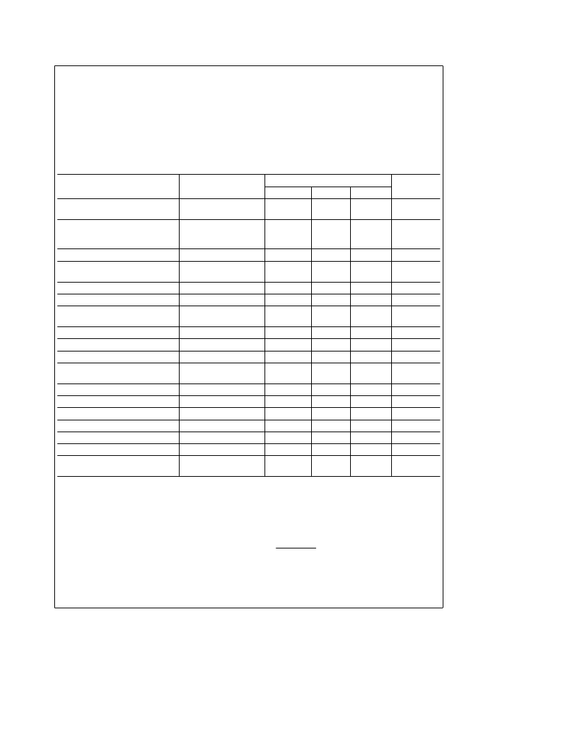
Absolute Maximum Ratings
If Military/Aerospace specified devices are required,
please contact the National Semiconductor Sales
Office/Distributors for availability and specifications.
Power Supply Voltage
26V
Power Dissipation (Note 1)
1000 mW
0
§
C to
a
70
§
C
a
260
§
C
Operating Temperature Range, LM566CN
Lead Temperature (Soldering, 10 sec.)
Electrical Characteristics
V
CC
e
12V, T
A
e
25
§
C, AC Test Circuit
Parameter
Conditions
LM566C
Units
Min
Typ
Max
Maximum Operating
Frequency
R0
e
2k
C0
e
2.7 pF
0.5
1
MHz
VCO Free-Running
Frequency
C
O
e
1.5 nF
R
O
e
20k
f
O
e
10 kHz
b
30
0
a
30
%
Input Voltage Range Pin 5
*/4
V
CC
V
CC
Average Temperature Coefficient
of Operating Frequency
200
ppm/
§
C
Supply Voltage Rejection
10–20V
0.1
2
%/V
Input Impedance Pin 5
0.5
1
M
X
VCO Sensitivity
For Pin 5, From
8–10V, f
O
e
10 kHz
6.0
6.6
7.2
kHz/V
FM Distortion
g
10% Deviation
0.2
1.5
%
Maximum Sweep Rate
1
MHz
Sweep Range
10:1
Output Impedance
Pin 3
50
X
Pin 4
50
X
Square Wave Output Level
R
L1
e
10k
5.0
5.4
Vp-p
Triangle Wave Output Level
R
L2
e
10k
2.0
2.4
Vp-p
Square Wave Duty Cycle
40
50
60
%
Square Wave Rise Time
20
ns
Square Wave Fall Time
50
ns
Triangle Wave Linearity
a
1V Segment at
(/2
V
CC
0.5
%
Note 1:
The maximum junction temperature of the LM566CN is 150
§
C. For operation at elevated junction temperatures, maximum power dissipation must be
derated based on a thermal resistance of 115
§
C/W, junction to ambient.
Applications Information
The LM566CN may be operated from either a single supply
as shown in this test circuit, or from a split (
g
) power sup-
ply. When operating from a split supply, the square wave
output (pin 3) is TTL compatible (2 mA current sink) with the
addition of a 4.7 k
X
resistor from pin 3 to ground.
A 0.001
m
F capacitor is connected between pins 5 and 6 to
prevent parasitic oscillations that may occur during VCO
switching.
f
O
e
2.4(V
a
b
V
5
)
R
O
C
O
V
a
where
2K
k
R
O
k
20K
and V
5
is voltage between pin 5 and pin 1.
2
相關PDF資料 |
PDF描述 |
|---|---|
| LM566CN | LM566C Voltage Controlled Oscillator |
| LM56 | Aluminum Electrolytic Capacitor; Capacitor Type:High Temperature; Voltage Rating:40VDC; Capacitor Dielectric Material:Aluminum Electrolytic; Operating Temperature Range:-55 C to +125 C; Capacitance:680uF RoHS Compliant: Yes |
| LM56BIM | Dual Output Low Power Thermostat |
| LM56BIMM | Dual Output Low Power Thermostat |
| LM56BIMMX | Dual Output Low Power Thermostat |
相關代理商/技術參數 |
參數描述 |
|---|---|
| LM566CN | 制造商:n/a 功能描述:_ 制造商:Texas Instruments 功能描述: |
| LM566CN/A+ | 制造商:未知廠家 制造商全稱:未知廠家 功能描述:Waveform Generator/Support |
| LM566CN/B+ | 制造商:未知廠家 制造商全稱:未知廠家 功能描述:Waveform Generator/Support |
| LM567 | 制造商:NSC 制造商全稱:National Semiconductor 功能描述:Tone Decoder |
| LM567 WAF | 制造商:Texas Instruments 功能描述: |
發布緊急采購,3分鐘左右您將得到回復。