- 您現在的位置:買賣IC網 > PDF目錄361030 > LM6041IN (NATIONAL SEMICONDUCTOR CORP) CONNECTOR PDF資料下載
參數資料
| 型號: | LM6041IN |
| 廠商: | NATIONAL SEMICONDUCTOR CORP |
| 元件分類: | 運算放大器 |
| 英文描述: | CONNECTOR |
| 中文描述: | OP-AMP, 6300 uV OFFSET-MAX, 0.075 MHz BAND WIDTH, PDIP8 |
| 封裝: | PLASTIC, DIP-8 |
| 文件頁數: | 2/12頁 |
| 文件大小: | 381K |
| 代理商: | LM6041IN |
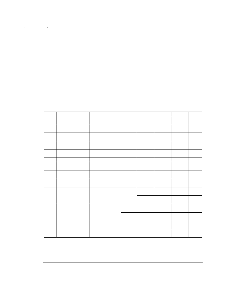
Absolute Maximum Ratings
(Note 1)
If Military/Aerospace specified devices are required,
please contact the National Semiconductor Sales Office/
Distributors for availability and specifications.
Differential Input Voltage
Supply Voltage (V
+
V
)
Output Short Circuit to V
Output Short Circuit to V
+
Lead Temperature
(Soldering, 10 sec.)
Storage Temperature Range
Junction Temperature
ESD Tolerance (Note 4)
Current at Input Pin
±
Supply Voltage
16V
(Note 2)
(Note 11)
260C
65C to +150C
110C
500V
±
5 mA
Current at Output Pin
Current at Power Supply Pin
Voltage at Input/Output Pin
Power Dissipation
±
18 mA
35 mA
(V
+
) + 0.3V, (V
) 0.3V
(Note 3)
Operating Ratings
Temperature Range
LMC6041AI, LMC6041I
Supply Voltage
Power Dissipation
Thermal Resistance (
θ
JA
) (Note 10)
8-Pin DIP
8-Pin SO
40C
≤
T
J
≤
+85C
4.5V
≤
V
+
≤
15.5V
(Note 9)
101C/W
165C/W
Electrical Characteristics
Unless otherwise specified, all limits guaranteed for T
= T
= 25C.
Boldface
limits apply at the temperature extremes. V
+
=
5V, V
= 0V, V
CM
= 1.5V, V
O
= V
+
/2, and R
L
1M unless otherwise specified.
Typical
(Note 5)
LMC6041AI
Limit
(Note 6)
LMC6041I
Limit
(Note 6)
6
6.3
Units
(Limit)
Symbol
Parameter
Conditions
V
OS
Input Offset Voltage
1
3
mV
max
μV/C
3.3
TCV
OS
Input Offset Voltage
Average Drift
Input Bias Current
1.3
I
B
0.002
4
4
pA
max
pA
max
Tera
dB
min
dB
min
dB
min
V
max
V
min
V/mV
min
V/mV
min
V/mV
min
V/mV
min
I
OS
Input Offset Current
0.001
2
2
R
IN
CMRR
Input Resistance
Common Mode
Rejection Ratio
Positive Power Supply
Rejection Ratio
Negative Power Supply
Rejection Ratio
Input Common-Mode
Voltage Range
>
10
75
0V
≤
V
CM
≤
12.0V
V
+
= 15V
5V
≤
V
+
≤
15V
V
O
= 2.5V
0V
≤
V
≤
10V
V
O
= 2.5V
V
+
= 5V and 15V
for CMRR
≥
50 dB
68
66
68
66
84
83
0.1
0
62
60
62
60
74
73
0.1
0
+PSRR
75
PSRR
94
CMR
0.4
V
+
1.9V
V
+
2.3V
V
+
2.5V
400
300
180
120
200
160
100
60
V
+
2.3V
V
+
2.4V
300
200
90
70
100
80
50
40
A
V
Large Signal
Voltage Gain
R
L
= 100 k
(Note 7)
Sourcing
1000
Sinking
500
R
L
= 25 k
(Note 7)
Sourcing
1000
Sinking
250
www.national.com
2
相關PDF資料 |
PDF描述 |
|---|---|
| LMC6041 | CMOS Single Micropower Operational Amplifier |
| LMC6041AIM | CMOS Single Micropower Operational Amplifier |
| LMC6041AIN | CMOS Single Micropower Operational Amplifier |
| LMC6041IM | CMOS Single Micropower Operational Amplifier |
| LM604 | 4 CHANNEL MUX-AMP |
相關代理商/技術參數 |
參數描述 |
|---|---|
| LM604ACM | 制造商:Rochester Electronics LLC 功能描述:- Bulk |
| LM604ACN | 制造商:NSC 制造商全稱:National Semiconductor 功能描述:4 CHANNEL MUX-AMP |
| LM604AMJ | 制造商:NSC 制造商全稱:National Semiconductor 功能描述:4 CHANNEL MUX-AMP |
| LM604AMJ-MIL | 制造商:未知廠家 制造商全稱:未知廠家 功能描述:Voltage-Feedback Operational Amplifier |
| LM604CM | 制造商:Rochester Electronics LLC 功能描述:- Bulk |
發布緊急采購,3分鐘左右您將得到回復。