- 您現在的位置:買賣IC網 > PDF目錄361031 > LM611 (National Semiconductor Corporation) 2.54mm CGrid Hdr Shrd /Slt .76AuLF 20Ckt RoHS Compliant: Yes PDF資料下載
參數資料
| 型號: | LM611 |
| 廠商: | National Semiconductor Corporation |
| 英文描述: | 2.54mm CGrid Hdr Shrd /Slt .76AuLF 20Ckt RoHS Compliant: Yes |
| 中文描述: | 運算放大器和可調參考 |
| 文件頁數: | 4/17頁 |
| 文件大小: | 735K |
| 代理商: | LM611 |
Electrical Characteristics
(Continued)
These specifications apply for V
= GND = 0V, V
+
= 5V, V
= V
= 2.5V, I
R
= 100 μA, FEEDBACK pin shorted to GND,
unless otherwise specified. Limits in standard typeface are for T
J
= 25C; limits in
boldface type
apply over the
Operating
Temperature Range.
LM611M
LM611BI
LM611I
LM611C
Limits
(Note 6)
LM611AM
LM611AI
Limits
(Note 6)
Symbol
Parameter
Conditions
Typical
(Note 5)
Units
VOLTAGE REFERENCE
V
R
Change with
V
ANODE
Change
V
+
= V
+
max,
V
R
= V
R
(
@
V
ANODE
= V
= GND) V
R
(
@
V
ANODE
= V
+
1.0V)
I
FB
; V
ANODE
≤
V
FB
≤
5.06V
0.7
3.3
22
29
30
1.5
3.0
35
40
1.6
3.0
50
55
mV max
mV max
nA max
nA max
μV
RMS
I
FB
FEEDBACK Bias
Current
V
R
Noise
e
n
10 Hz to 10,000 Hz, V
RO
= V
R
Note 1:
Absolute maximum ratings indicate limits beyond which damage to the component may occur. Electrical specifications do not apply when operating the de-
vice beyond its rated operating conditions.
Note 2:
More accurately, it is excessive current flow, with resulting excess heating, that limits the voltages on all pins. When any pin is pulled a diode drop below
V
, a parasitic NPN transistor turns ON. No latch-up will occur as long as the current through that pin remains below the Maximum Rating. Operation is undefined
and unpredictable when any parasitic diode or transistor is conducting.
Note 3:
Junction temperature may be calculated using T
=T
+ P
θ
. The given thermal resistance is worst-case for packages in sockets in still air. For packages
soldered to copper-clad board with dissipation from one op amp or reference output transistor, nominal
θ
JA
is 90C/W for the N package and 135C/W for the M pack-
age.
Note 4:
Human body model, 100 pF discharged through a 1.5 k
resistor.
Note 5:
Typical values in standard typeface are for T
J
= 25C; values in
boldface type
apply for the full operating temperature range. These values represent the
most likely parametric norm.
Note 6:
All limits are guaranteed at room temperature (standard type face) or at operating temperature extremes
(bold face type)
.
Note 7:
Slew rate is measured with op amp in a voltage follower configuration. For rising slew rate, the input voltage is driven from 5V to 25V, and the output voltage
transition is sampled at 10V and 20V. For falling slew rate, the input voltage is driven from 25V to 5V, and output voltage transition is sampled at 20V and 10V.
Note 8:
V
R
is the cathode-feedback voltage, nominally 1.244V.
Note 9:
Average reference drift is calculated from the measurement of the reference voltage at 25C and at the temperature extremes. The drift, in ppm/C, is
10
V
/(V
T
), where
V
is the lowest value subtracted from the highest, V
R[25C]
is the value at 25C, and
T
J
is the temperature range. This parameter
is guaranteed by design and sample testing.
Note 10:
Hysteresis is the change in V
caused by a change in T
, after the reference has been “dehysterized”. To dehysterize the reference; that is minimize the
hysteresis to the typical value, its junction temperature should be cycled in the following pattern, spiraling in toward 25C: 25C, 85C, 40C, 70C, 0C, 25C.
Note 11:
Low contact resistance is required for accurate measurement.
Note 12:
Military RETS 611AMX electrical test specification is available on request. The LM611AMJ/883 can also be procured as a Standard Military Drawing.
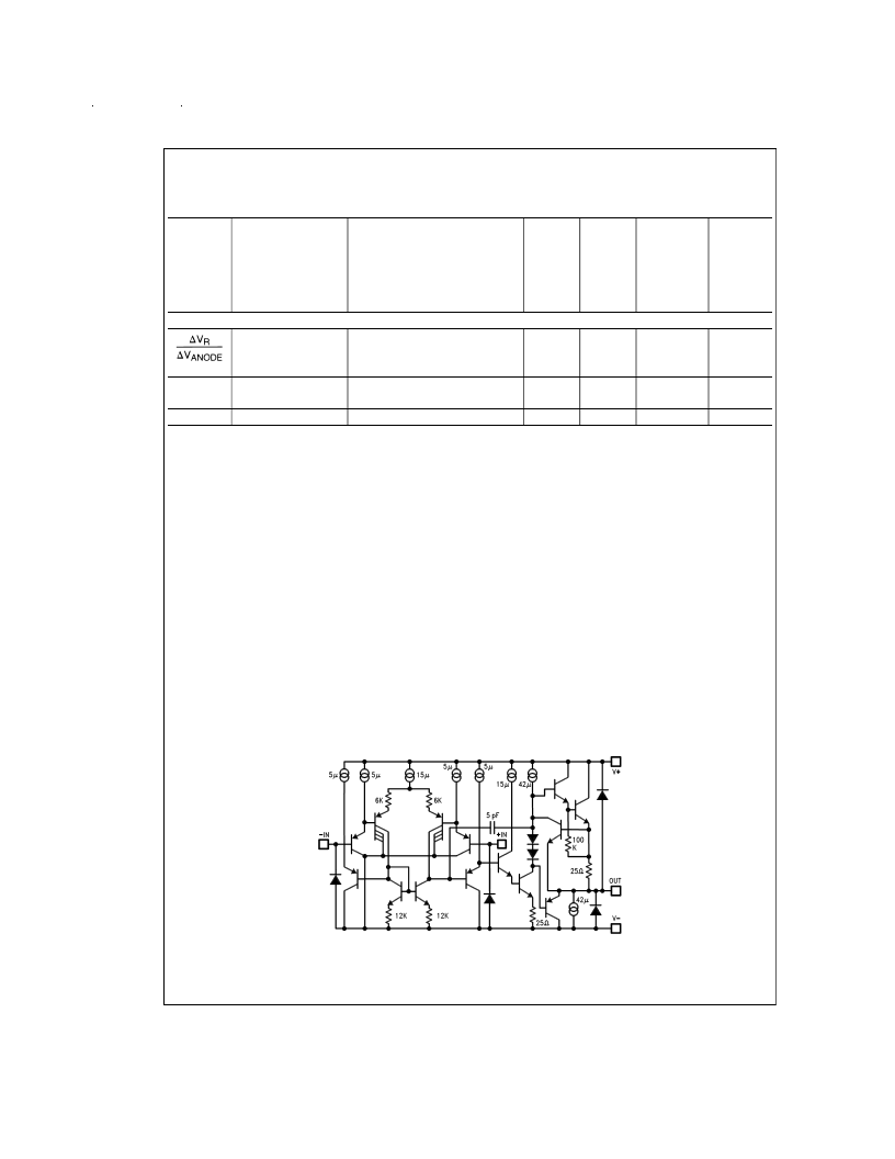
Simplified Schematic Diagrams
Op Amp
DS009221-3
www.national.com
4
相關PDF資料 |
PDF描述 |
|---|---|
| LM611D-SERIES | Optoelectronic |
| LM611IMX | Voltage-Feedback Operational Amplifier |
| LM611IN | Voltage-Feedback Operational Amplifier |
| LM611MJ | Voltage-Feedback Operational Amplifier |
| LM6118H | Voltage-Feedback Operational Amplifier |
相關代理商/技術參數 |
參數描述 |
|---|---|
| LM6118 | 制造商:NSC 制造商全稱:National Semiconductor 功能描述:Fast Settling Dual Operational Amplifiers |
| LM6118H | 制造商:未知廠家 制造商全稱:未知廠家 功能描述:Voltage-Feedback Operational Amplifier |
| LM6118J | 制造商:未知廠家 制造商全稱:未知廠家 功能描述:Voltage-Feedback Operational Amplifier |
| LM6118J/883 | 制造商:Texas Instruments 功能描述:OP Amp Dual GP ±20V 8-Pin CDIP |
| LM6118J/883 WAF | 制造商:Texas Instruments 功能描述: |
發布緊急采購,3分鐘左右您將得到回復。